Chapter: Microprocessor and Microcontroller
Basic 8051 Architecture
Basic 8051 Architecture
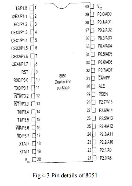
The 8051 is an 8-bit microcontroller i.e. the data bus within and outside the chip is eight bits wide. The address bus of the 8051 is 16-bit wide. So it can address 64 KB of memory. The 8051 is a 40-pin chip as shown is figure below:
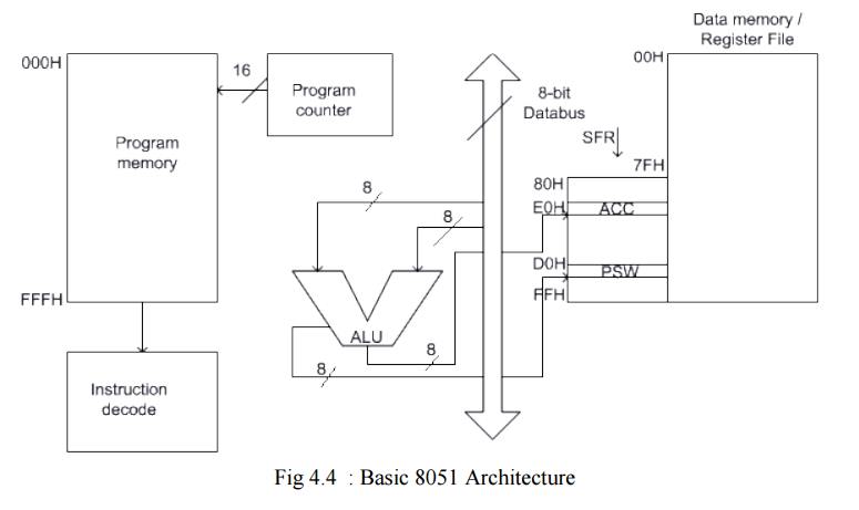
8051 employs Harvard architecture. It has some peripherals such as 32 bit digital I/O, Timers and Serial I/O. The basic architecture of 8051 is given in fig 4.4.
Various features of 8051 microcontroller are given as follows.
· 8-bit CPU
· 16-bit Program Counter
· 8-bit Processor Status Word (PSW)
· 8-bit Stack Pointer
· Internal RAM of 128bytes
· Special Function Registers (SFRs) of 128 bytes
· 32 I/O pins arranged as four 8-bit ports (P0 - P3)
· Two 16-bit timer/counters : T0 and T1
· Two external and three internal vectored interrupts
· One full duplex serial I/O
8051 Clock and Instruction Cycle
In 8051, one instruction cycle consists of twelve (12) clock cycles. Instruction cycle is sometimes called as Machine cycle by some authors.
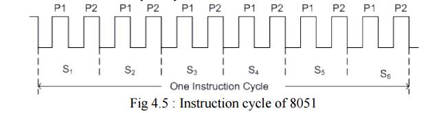
In 8051, each instruction cycle has six states (S 1 - S 6 ). Each state has two pulses (P1 and P2)
128 bytes of Internal RAM Structure (lower address space)
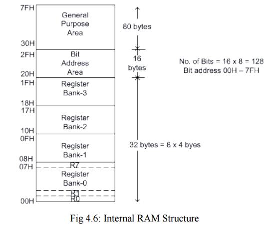
The lower 32 bytes are divided into 4 separate banks. Each register bank has 8 registers of one byte each. A register bank is selected depending upon two bank select bits in the PSW register. Next 16bytes are bit addressable. In total, 128bits (16X8) are available in bitaddressable area. Each bit can be accessed and modified by suitable instructions. The bit addresses are from 00H (LSB of the first byte in 20H) to 7FH (MSB of the last byte in 2FH). Remaining 80bytes of RAM are available for general purpose.
Internal Data Memory and Special Function Register (SFR) Map
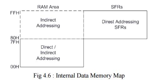
The special function registers (SFRs) are mapped in the upper 128 bytes of internal data memory address. Hence there is an address overlap between the upper 128 bytes of data RAM and SFRs. Please note that the upper 128 bytes of data RAM are present only in the 8052 family. The lower128 bytes of RAM (00H - 7FH) can be accessed both by direct or indirect addressing while the upper 128 bytes of RAM (80H - FFH) are accessed by indirect addressing.The SFRs (80H - FFH) are accessed by direct addressing only. This feature distinguishes the upper 128 bytes of memory from the SFRs, as shown in fig 4.6.
SFR Map
The set of Special Function Registers (SFRs) contains important registers such as Accumulator, Register B, I/O Port latch registers, Stack pointer, Data Pointer, Processor Status Word (PSW) and various control registers. Some of these registers are bit addressable (they are marked with a * in the diagram below). The detailed map of various registers is shown in the following figure.
Address
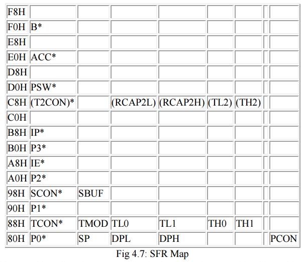
It should be noted hat all registers appearing in the first column are bit addressable. The bit address of a bit in the register is calculated as follows.
Bit address of 'b' bit of register 'R' is Address of register 'R' + b where 0 ≤ b ≤ 7
Processor Status Word (PSW) Address=D0H
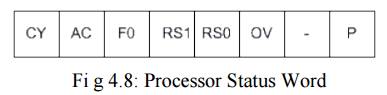
PSW register stores the important status conditions of the microcontroller. It also stores the bank select bits (RS1 & RS0) for register bank selection.
Interfacing External Memory
If external program/data memory are to be interfaced, they are interfaced in the following way.
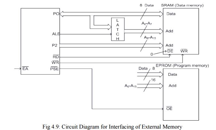
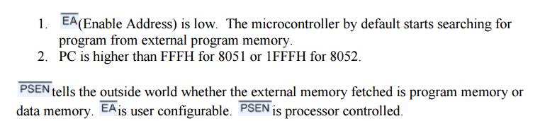
External program memory is fetched if either of the following two conditions are satisfied.
8051 Addressing Modes
8051 has four addressing modes.
1. Immediate Addressing :
Data is immediately available in the instruction. For example -
ADD A, #77; Adds 77 (decimal) to A and stores in A
ADD A, #4DH; Adds 4D (hexadecimal) to A and stores in A
MOV DPTR, #1000H; Moves 1000 (hexadecimal) to data pointer 2. Bank Addressing or Register Addressing :
This way of addressing accesses the bytes in the current register bank. Data is available in the register specified in the instruction. The register bank is decided by 2 bits of Processor Status Word (PSW).
For example-
ADD A, R0; Adds content of R0 to A and stores in A
3.. Direct Addressing :
The address of the data is available in the instruction. For example -
MOV A, 088H; Moves content of SFR TCON (address 088H)to A 4. Register Indirect Addressing :
The address of data is available in the R0 or R1 registers as specified in the instruction. For example -
MOV A, @R0 moves content of address pointed by R0 to A External Data Addressing :
Pointer used for external data addressing can be either R0/R1 (256 byte access) or DPTR (64kbyte access).
For example -
MOVX A, @R0; Moves content of 8-bit address pointed by R0 to A
MOVX A, @DPTR; Moves content of 16-bit address pointed by DPTR to A External Code Addressing :
Sometimes we may want to store non-volatile data into the ROM e.g. look-up tables. Such data may require reading the code memory. This may be done as follows -
MOVC A, @A+DPTR; Moves content of address pointed by A+DPTR to A
MOVC A, @A+PC; Moves content of address pointed by A+PC to A
Related Topics