Chapter: Microprocessor and Microcontroller
8257: Direct Memory Access Controller
8257: Direct Memory Access Controller
The Direct Memory Access or DMA mode of data
transfer is the fastest amongst all the modes of data transfer. In this mode,
the device may transfer data directly to/from memory without any interference
from the CPU. The device requests the CPU (through a DMA controller) to hold
its data, address and control bus, so that the device may transfer data
directly to/from memory.
The DMA
data transfer is initiated only after receiving HLDA signal from the CPU.
Intel’s 8257 is a four channel DMA controller designed to be interfaced with
their family of microprocessors. The 8257, on behalf of the devices, requests
the CPU for bus access using local bus request input i.e. HOLD in minimum mode.
In maximum mode of the microprocessor RQ/GT pin is used as bus request input.
On
receiving the HLDA signal (in minimum mode) or RQ/GT signal (in maximum mode)
from the CPU, the requesting devices gets the access of the bus, and it
completes the required number of DMA cycles for the data transfer and then
hands over the control of the bus back to the CPU.
Internal Architecture of 8257
The
internal architecture of 8257 is shown in figure. The chip support four DMA
channels, i.e. four peripheral devices can independently request for DMA data
transfer through these channels at a time. The DMA controller has 8-bit
internal data buffer, a read/write unit, a control unit, a priority resolving
unit along with a set of registers.
Register Organization of 8257
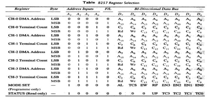
The 8257
performs the DMA operation over four independent DMA channels. Each of four
channels of 8257 has a pair of two 16-bit registers, viz. DMA address
register and terminal count
register.
There are
two common registers for all the channels, namely, mode set register and status
register. Thus there are a total of
ten registers. The CPU selects one of these ten registers using address lines Ao-A3. Table shows how the Ao-A3 bits may be
used for selecting one of these registers.
DMA Address Register
Each DMA
channel has one DMA address register. The function of this register is to store
the address of the starting memory location, which will be accessed by the DMA
channel. Thus the starting address of the memory block which will be accessed
by the device is first loaded in the DMA address register of the channel.
The
device that wants to transfer data over a DMA channel, will access the block of
the memory with the starting address stored in the DMA Address Register.
Terminal Count Register
Each of the
four DMA channels of 8257 has one terminal count register (TC). This 16-bit
register isused for ascertaining that the data transfer through a DMA channel
ceases or stops after the required number of DMA cycles. The low order 14-bits
of the terminal count register are initialised with the binary equivalent of
the number of required DMA cycles minus one.
After
each DMA cycle, the terminal count register content will be decremented by one
and finally it becomes zero after the required number of DMA cycles are over.
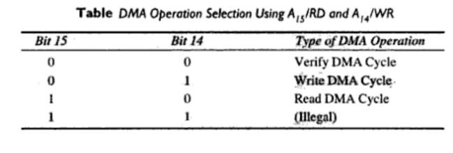
The bits 14 and 15 of this register indicate the type of the DMA operation
(transfer). If the device wants to write data into the memory, the DMA
operation is called DMA write operation. Bit 14 of the register in this case
will be set to one and bit 15 will be set to zero.
Table
gives detail of DMA operation selection and corresponding bit configuration of
bits 14 and 15 of the TC register.
Mode Set Register
The mode
set register is used for programming the 8257 as per the requirements of the
system. The function of the mode set register is to enable the DMA channels
individually and also to set the various modes of operation.
The DMA
channel should not be enabled till the DMA address register and the terminal
count register contain valid information, otherwise, an unwanted DMA request
may initiate a DMA cycle, probably destroying the valid memory data. The bits
Do-D3 enable one of the four DMA channels of 8257. for example, if Do is ‘1’,
channel 0 is enabled. If bit 4 is set, rotating priority is enabled, otherwise,
the normal, i.e. fixed priority is enabled.
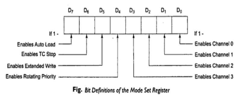
If the TC
STOP bit is set, the selected channel is disabled after the terminal count condition is reached, and
it further prevents any DMA cycle on the channel. To enable the channel again,
this bit must be reprogrammed. If the TC STOP bit is programmed to be zero, the
channel is not disabled, even after the count reaches zero and further request
are allowed on the same channel.
The auto
load bit, if set, enables channel 2 for the repeat block chaining operations,
without immediate software intervention between the two successive blocks. The
channel 2 registers are used as usual, while the channel 3 registers are used
to store the block reinitialisation parameters, i.e. the DMA starting address
and terminal count. After the first block is transferred using DMA, the channel
2 registers are reloaded with the corresponding channel 3 registers for the
next block transfer, if the update
flag is set. The extended write bit, if set to ‘1’, extends the duration of
MEMW and IOW signals by activating them earlier, this is useful in interfacing
the peripherals with different access times.
If the
peripheral is not accessed within the stipulated time, it is expected to give
the ‘NOT READY’ indication to 8257, to request it to add one or more wait
states in the DMA CYCLE. The mode set register can only be written into.
Status Register
The
status register of 8257 is shown in figure. The lower order 4-bits of this
register contain the terminal count status for the four individual channels. If
any of these bits is set, it indicates that the specific channel has reached
the terminal count condition.
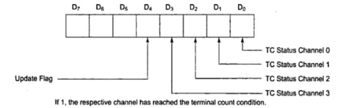
These
bits remain set till either the status is read by the CPU or the 8257 is reset.
The update flag is not affected by the read operation. This flag can only be
cleared by resetting 8257 or by resetting the auto load bit of the mode set
register. If the update flag is set, the contents of the channel 3 registers
are reloaded to the corresponding registers of channel 2 whenever the channel 2
reaches a terminal count condition, after transferring one block and the next
block is to be transferred using the autoload feature of 8257.
The update
flag is set every time, the channel 2 registers are loaded with contents of the
channel 3 registers. It is cleared by the completion of the first DMA cycle of
the new block. This register can only read.
Data Bus Buffer, Read/Write Logic, Control Unit and
Priority Resolver
The
8-bit. Tristate, bidirectional buffer interfaces the internal bus of 8257 with
the external system bus under the control of various control signals.
In the
slave mode, the read/write logic accepts the I/O Read or I/O Write signals,
decodes the Ao-A3 lines and either writes the contents of the data bus to the
addressed internal register or reads the contents of the selected register
depending upon whether IOW or IOR signal is activated.
In master
mode, the read/write logic generates the IOR and IOW signals to control the
data flow to or from the selected peripheral. The control logic controls the
sequences of operations and generates the required control signals like AEN,
ADSTB, MEMR, MEMW, TC and MARK along with the address lines A4-A7, in master
mode. The priority resolver resolves the priority of the four DMA channels
depending upon whether normal priority or rotating priority is programmed.
Signal Description of 8257
DRQo-DRQ3 :
These are
the four individual channel DMA request inputs, used by the peripheral devices
for requesting the DMA services. The DRQo has the highest priority while DRQ3 has the lowest one, if the fixed
priority mode is selected.
DACKo-DACK3 :
These are
the active-low DMA acknowledge output lines which inform the requesting
peripheral that the request has been honoured and the bus is relinquished by
the CPU. These lines may act as strobe lines for the requesting devices.
Do-D7:
These are
bidirectional, data lines used to interface the system bus with the internal
data bus of 8257. These lines carry command words to 8257 and status word from
8257, in slave mode, i.e. under the control of CPU.
The data
over these lines may be transferred in both the directions. When the 8257 is
the bus master (master mode, i.e. not under CPU control), it uses Do-D7 lines
to send higher byte of the generated address to the latch. This address is
further latched using ADSTB signal. the address is transferred over Do-D7 during
the first clock cycle of the DMA cycle. During the rest of the period, data is
available on the data bus.
IOR:
This is
an active-low bidirectional tristate input line that acts as an input in the
slave mode. In slave mode, this input signal is used by the CPU to read
internal registers of 8257.this line acts output in master mode. In master
mode, this signal is used to read data from a peripheral during a memory write
cycle.
IOW :
This is
an active low bidirection tristate line that acts as input in slave mode to
load the contents of the data bus to the 8-bit mode register or upper/lower
byte of a 16-bit DMA address register or terminal count register. In the master
mode, it is a control output that loads the data to a peripheral during DMA
memory read cycle (write to peripheral).
CLK:
This is a
clock frequency input required to derive basic system timings for the internal
operation of 8257.
RESET :
This
active-high asynchronous input disables all the DMA channels by clearing the
mode register and tristates all the control lines.
Ao-A3:
These are
the four least significant address lines. In slave mode, they act as input
which select one of the registers to be read or written. In the master mode,
they are the four least significant memory address output lines generated by
8257.
CS:
This is
an active-low chip select line that enables the read/write operations from/to
8257, in slave mode. In the master mode, it is automatically disabled to
prevent the chip from getting selected (by CPU) while performing the DMA
operation.
A4-A7 :
This is
the higher nibble of the lower byte address generated by 8257 during the master
mode of DMA operation.
READY:
This is
an active-high asynchronous input used to stretch memory read and write cycles
of 8257 by inserting wait states. This is used while interfacing slower
peripherals..
HRQ:
The hold
request output requests the access of the system bus. In the non-cascaded 8257
systems, this is connected with HOLD pin of CPU. In the cascade mode, this pin
of a slave is connected with a DRQ input line of the master 8257, while that of
the master is connected with HOLD input of the CPU.
HLDA :
The CPU
drives this input to the DMA controller high, while granting the bus to the
device. This pin is connected to the HLDA output of the CPU. This input, if
high, indicates to the DMA controller that the bus has been granted to the
requesting peripheral by the CPU.
MEMR:
This
active –low memory read output is used to read data from the addressed memory
locations during DMA read cycles.
MEMW :
This
active-low three state output is used to write data to the addressed memory
location during DMA write operation.
ADST :
This
output from 8257 strobes the higher byte of the memory address generated by the
DMA controller into the latches.
AEN:
This
output is used to disable the system data bus and the control the bus driven by
the CPU, this may be used to disable the system address and data bus by using
the enable input of the bus drivers to inhibit the non-DMA devices from
responding during DMA operations. If the 8257 is I/O mapped, this should be
used to disable the other I/O devices, when the DMA controller addresses is on
the address bus.
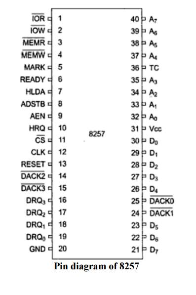
TC:
Terminal
count output indicates to the currently selected peripherals that the present
DMA cycle is the last for the previously programmed data block. If the TC STOP
bit in the mode set register is set, the selected channel will be disabled at
the end of the DMA cycle.
The TC
pin is activated when the 14-bit content of the terminal count register of the
selected channel becomes equal to zero. The lower order 14 bits of the terminal
count register are to be programmed with a 14-bit equivalent of (n-1), if n is
the desired number of DMA cycles.
MARK :
The
modulo 128 mark output indicates to the selected peripheral that the current
DMA cycle
is the 128th cycle since the previous MARK output. The mark will be
activated after each 128 cycles or integral multiples of it from the beginning
if the data block (the first DMA cycle), if the total number of the required
DMA cycles (n) is completely divisible by 128.
Vcc :
This is a
+5v supply pin required for operation of the circuit.
GND :
This is a
return line for the supply (ground pin of the IC).
Interfacing 8257 with 8086
Once a
DMA controller is initialised by a CPU property, it is ready to take control of
the system bus on a DMA request, either from a peripheral or itself (in case of
memory-to-memory transfer). The DMA controller sends a HOLD request to the CPU
and waits for the CPU to assert the HLDA signal. The CPU relinquishes the
control of the bus before asserting the HLDA signal.
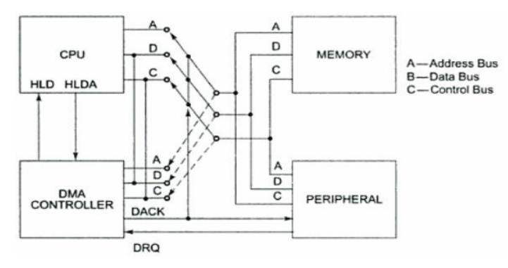
A
conceptual implementation of the system is shown in Figure
Once the
HLDA signal goes high, the DMA controller activates the DACK signal to the
requesting peripheral and gains the control of the system bus. The DMA
controller is the sole master of the bus, till the DMA operation is over. The
CPU remains in the HOLD status (all of its signals are tristate except HOLD and
HLDA), till the DMA controller is the master of the bus.
In other
words, the DMA controller interfacing circuit implements a switching
arrangement for the address, data and control busses of the memory and
peripheral subsystem from/to the CPU to/from the DMA controller.
Related Topics