Chapter: Microprocessor and Microcontroller
8086 Microprocessor Architecture and Operation
8086 Microprocessor Architecture and Operation:
It is a
16 bit µp. 8086 has a 20 bit address bus can access upto 220 memory locations (
1 MB) . It can support upto 64K I/O ports. It provides 14, 16-bit registers. It
has multiplexed address and data bus AD0- AD15 and A16 – A19. It requires
single phase clock with 33% duty cycle to provide internal timing. 8086 is
designed to operate in two modes, Minimum and Maximum. It can prefetches upto 6
instruction bytes from memory and queues them in order to speed up instruction
execution. It requires +5V power supply. A 40 pin dual in line package.
Minimum and Maximum Modes:
The
minimum mode is selected by applying logic 1 to the MN / MX# input pin. This is
a single microprocessor configuration. The maximum mode is selected by applying
logic 0 to the MN / MX# input pin. This is a multi micro processors
configuration.
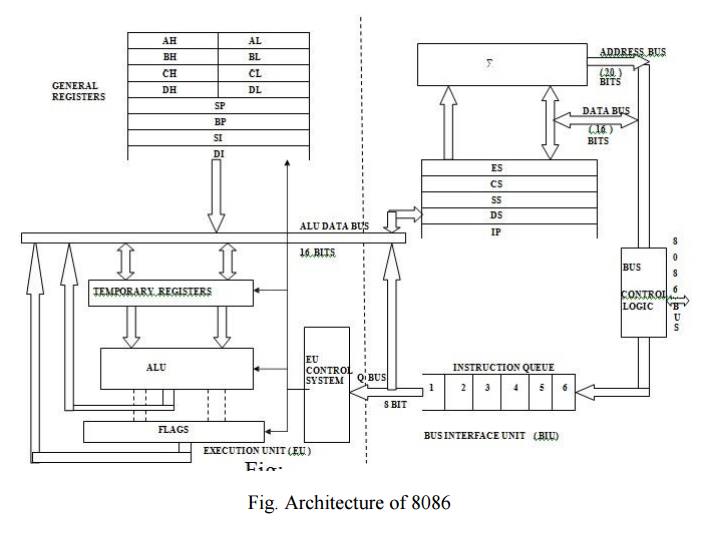
Internal
Architecture of 8086
8086 has
two blocks BIU and EU. The BIU performs all bus operations such as instruction
fetching, reading and writing operands for memory and calculating the addresses
of the memory operands. The instruction bytes are transferred to the
instruction queue. EU executes instructions from the instruction system byte
queue. Both units operate asynchronously to give the 8086 an overlapping
instruction fetch and execution mechanism which is called as Pipelining. This
results in efficient use of the system bus and system performance. BIU contains
Instruction queue, Segment registers, Instruction pointer, Address adder. EU
contains Control circuitry, Instruction decoder, ALU, Pointer and Index
register, Flag register.
Bus
Interfacr Unit:
It
provides a full 16 bit bidirectional data bus and 20 bit address bus. The bus
interface unit is responsible for performing all external bus operations.
Specifically
it has the following functions:
Instruction
fetch, Instruction queuing, Operand fetch and storage, Address relocation and
Bus control. The BIU uses a mechanism known as an instruction stream queue to
implement a pipeline architecture.
This
queue permits prefetch of up to six bytes of instruction code. When ever the
queue of the BIU is not full, it has room for at least two more bytes and at
the same time the EU is not requesting it to read or write operands from
memory, the BIU is free to look ahead in the program by prefetching the next
sequential instruction. These prefetching instructions are held in its FIFO
queue. With its 16 bit data bus, the BIU fetches two instruction bytes in a
single memory cycle. After a byte is loaded at the input end of the queue, it
automatically shifts up through the FIFO to the empty location nearest the
output.
The EU
accesses the queue from the output end. It reads one instruction byte after the
other from the output of the queue. If the queue is full and the EU is not
requesting access to operand in memory. These intervals of no bus activity,
which may occur between bus cycles are known as Idle state. If the BIU is already in the process
of fetching an instruction when the EU request it to read or write operands
from memory or I/O, the BIU first completes the instruction fetch bus cycle
before initiating the operand read / write cycle. The BIU also contains a
dedicated adder which is used to generate the 20 bit physical address that is
output on the address bus. This address is formed by adding an appended 16 bit
segment address and a 16 bit offset address. For example, the physical address
of the next instruction to be fetched is formed by combining the current contents
of the code segment CS register and the current contents of the instruction
pointer IP register. The BIU is also responsible for generating bus control
signals such as those for memory read or write and I/O read or write.
EXECUTION UNIT : The Execution unit is
responsible for decoding and executing all
instructions. The EU extracts instructions from the top of the queue in the
BIU, decodes them, generates operands if necessary, passes them to the BIU and
requests it to perform the read or write bys cycles to memory or I/O and
perform the operation specified by the instruction on the operands. During the
execution of the instruction, the EU tests the status and control flags and
updates them based on the results of executing the instruction. If the queue is
empty, the EU waits for the next instruction byte to be fetched and shifted to
top of the queue. When the EU executes a branch or jump instruction, it
transfers control to a location corresponding to another set of sequential
instructions. Whenever this happens, the BIU automatically resets the queue and
then begins to fetch instructions from this new location to refill the queue.
Internal
Registers of 8086
The 8086
has four groups of the user accessible internal registers. They are the
instruction pointer, four data registers, four pointer and index register, four
segment registers.
The 8086
has a total of fourteen 16-bit registers including a 16 bit register called the
status
register,
with 9 of bits implemented for status and control flags. Most of the registers contain
data/instruction offsets within 64 KB memory segment. There are four different
64 KB segments for instructions, stack, data and extra data. To specify where
in 1 MB of processor memory these 4 segments are located the processor uses
four segment registers:
Code segment (CS) is a 16-bit register
containing address of 64 KB segment with processor instructions. The processor uses CS segment for all accesses to
instructions referenced by instruction pointer (IP) register. CS register
cannot be changed directly. The CS register is automatically updated during far
jump, far call and far return instructions.
Stack segment (SS) is a 16-bit register
containing address of 64KB segment with program stack. By default, the processor assumes that all data referenced
by the stack pointer (SP) and base pointer (BP) registers is located in the
stack segment. SS register can be changed directly using POP instruction.
Data segment (DS) is a 16-bit register
containing address of 64KB segment with program data. By default, the processor assumes that all data referenced
by general registers (AX, BX, CX, DX) and index register (SI, DI) is located in
the data segment. DS register can be changed directly using POP and LDS instructions.
Extra segment (ES) is a 16-bit register
containing address of 64KB segment, usually with program data. By default, the processor assumes that the DI
register references the ES segment in string manipulation instructions. ES
register can be changed directly using POP and LES instructions. It is possible
to change default segments used by general and index registers by prefixing
instructions with a CS, SS, DS or ES prefix.
All
general registers of the 8086 microprocessor can be used for arithmetic and
logic operations. The general registers are:
Accumulator register consists of two 8-bit
registers AL and AH, which can be combined
together and used as a 16-bit register AX. AL in this case contains the
low-order byte of the word, and AH contains the high-order byte. Accumulator
can be used for I/O operations and string manipulation.
Base register consists of two 8-bit
registers BL and BH, which can be combined together and used as a 16-bit register BX. BL in this case contains the
low-order byte of the word, and BH contains the high-order byte. BX register
usually contains a data pointer used for based, based indexed or register
indirect addressing.
Count register consists of two 8-bit
registers CL and CH, which can be combined together and used as a 16-bit register CX. When combined, CL register
contains the low-order byte of the word, and CH contains the high-order byte.
Count register can be used in Loop, shift/rotate instructions and as a counter
in string manipulation,.
Data register consists of two 8-bit
registers DL and DH, which can be combined together and used as a 16-bit register DX. When combined, DL register
contains the low-order byte of the word, and DH contains the high- order byte.
Data register can be used as a port number in I/O operations. In integer 32-bit
multiply and divide instruction the DX register contains high-order word of the
initial or resulting number.
The
following registers are both general and index registers:
Stack Pointer (SP) is a 16-bit register
pointing to program stack.
Base Pointer (BP) is a 16-bit register
pointing to data in stack segment. BP register is usually used for based, based indexed or register indirect
addressing.
Source Index (SI) is a 16-bit register. SI is
used for indexed, based indexed and register indirect addressing, as well as a source data address in string
manipulation instructions.
Destination Index (DI) is a
16-bit register. DI is used for indexed, based indexed and register indirect addressing, as well as a destination data
address in string manipulation instructions.
Other
registers:
Instruction Pointer (IP) is a
16-bit register.
Flags is a 16-bit register containing 9
one bit flags.
Overflow Flag (OF) - set if the result is too
large positive number, or is too small negative number to fit into destination operand.
Direction Flag (DF) - if set then string
manipulation instructions will auto-decrement index registers. If cleared then the index registers will be
auto-incremented.
Interrupt-enable Flag (IF) -
setting this bit enables maskable interrupts.
Single-step Flag (TF) - if set then single-step
interrupt will occur after the next instruction.
Sign Flag (SF) - set if the most
significant bit of the result is set.
Zero Flag (ZF) - set if the result is zero
Auxiliary carry Flag (AF) -
set if there was a carry from or borrow to bits 0-3 in the AL register.
Parity Flag (PF) - set if parity (the number
of "1" bits) in the low-order byte of the result is even.
Carry Flag (CF) - set if there was a carry
from or borrow to the most significant bit during last result calculation.
Addressing Modes
Implied - the data value/data address is
implicitly associated with the instruction.
Register - references the data in a
register or in a register pair.
Immediate - the data is provided in the
instruction.
Direct - the instruction operand
specifies the memory address where data is located.
Register indirect -
instruction specifies a register containing an address, where data is located. This addressing mode works
with SI, DI, BX and BP registers.
Based :- 8-bit or 16-bit instruction
operand is added to the contents of a base register (BX or BP), the resulting value is a pointer to location where data
resides.
Indexed :- 8-bit or 16-bit instruction
operand is added to the contents of an index register (SI or DI), the resulting value is a pointer to location where
data resides.
Based Indexed :- the contents of a base
register (BX or BP) is added to the contents of an index register (SI or DI), the resulting value is a pointer to
location where data resides.
Based Indexed with displacement :- 8-bit
or 16-bit instruction operand is added to the contents of a base register (BX or BP) and index register (SI or
DI), the resulting value is a pointer to location where data resides.
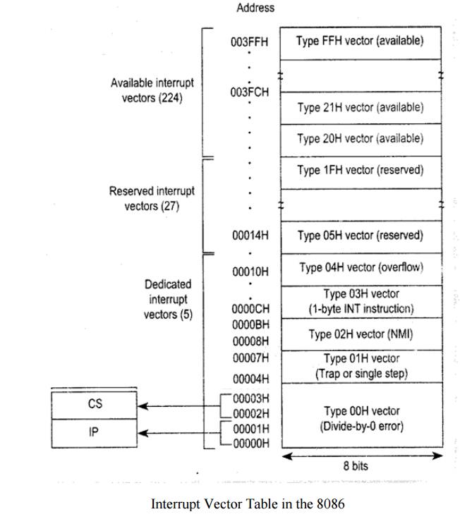
Interrupts
The
processor has the following interrupts:
INTR is a maskable hardware interrupt.
The interrupt can be enabled/disabled using
STI/CLI instructions or using more complicated method of updating the FLAGS
register with the help of the POPF instruction.
When an
interrupt occurs, the processor stores FLAGS register into stack, disables
further interrupts, fetches from the bus one byte representing interrupt type,
and jumps to interrupt processing routine address of which is stored in
location 4 * <interrupt type>. Interrupt processing routine should return
with the IRET instruction.
NMI is a non-maskable interrupt.
Interrupt is processed in the same way as the INTR interrupt. Interrupt type of the NMI is 2, i.e. the address of the
NMI processing routine is stored in location 0008h. This interrupt has higher
priority then the maskable interrupt.
Software interrupts can be
caused by:
INT
instruction - breakpoint interrupt. This is a type 3 interrupt.
INT
<interrupt number> instruction - any one interrupt from available 256
interrupts.
INTO
instruction - interrupt on overflow
Single-step
interrupt - generated if the TF flag is set. This is a type 1 interrupt. When
the CPU processes this interrupt it clears TF flag before calling the interrupt
processing routine.
Processor exceptions: Divide
Error (Type 0), Unused
Opcode
(type 6) and Escape opcode (type 7).
Software
interrupt processing is the same as for the hardware interrupts.
The
figure below shows the 256 interrupt vectors arranged in the interrupt vector
table in the memory.
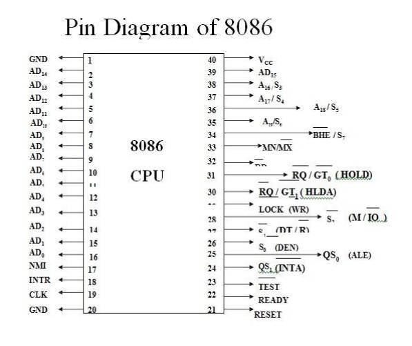
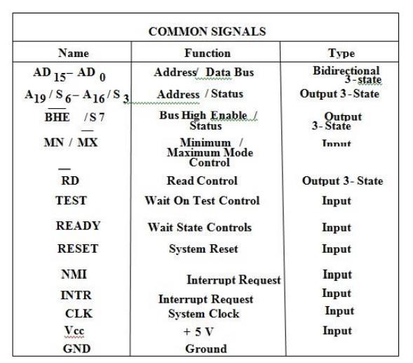
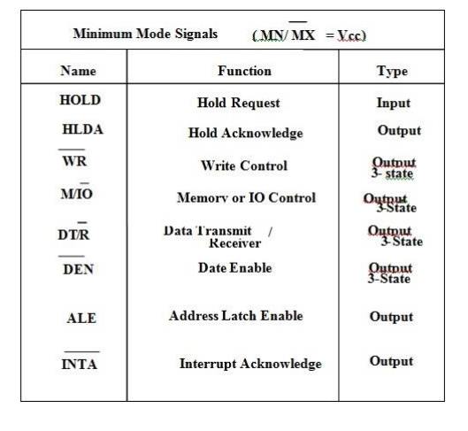
Minimum Mode Interface
When the
Minimum mode operation is selected, the 8086 provides all control signals
needed to implement the memory and I/O interface. The minimum mode signal can
be divided into the following basic groups : address/data bus, status, control,
interrupt and DMA.
Address/Data Bus : these lines serve two
functions. As an address bus is 20 bits long and consists of signal lines A0 through A19. A19 represents the MSB
and A0 LSB. A 20bit address gives the 8086 a 1Mbyte memory address space. More
over it has an independent I/O address space which is 64K bytes in length.
The 16
data bus lines D0 through D15 are actually multiplexed with address lines A0
through A15 respectively. By multiplexed we mean that the bus work as an
address bus during first machine cycle and as a data bus during next machine
cycles. D15 is the MSB and D0 LSB. When acting as a data bus, they carry
read/write data for memory, input/output data for I/O devices, and interrupt
type codes from an interrupt controller.
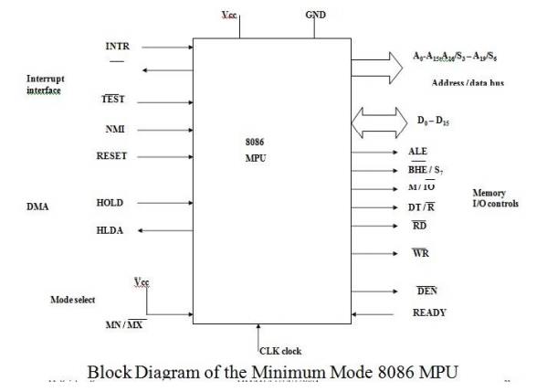
Status signal : The four most significant
address lines A19 through A16 are also multiplexed
but in this case with status signals S6 through S3. These status bits are
output on the bus at the same time that data are transferred over the other bus
lines. Bit S4 and S3 together from a 2 bit binary code that identifies which of
the 8086 internal segment registers are used to generate the physical address
that was output on the address bus during the current bus cycle. Code S4S3 = 00
identifies a register known as extra segment register as the source
of the segment address.
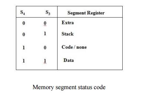
Memory
segment status code
Status
line S5 reflects the status of another internal characteristic of the 8086. It
is the logic level of the internal enable flag. The last status bit S6 is
always at the logic 0 level.
Control Signals : The control signals are
provided to support the 8086 memory I/O interfaces.
They control functions such as when the bus is to carry a valid address in
which direction data are to be transferred over the bus, when valid write data
are on the bus and when to put read data on the system bus.
ALE is a
pulse to logic 1 that signals external circuitry when a valid address word is
on the bus. This address must be latched in external circuitry on the 1-to-0
edge of the pulse at ALE.
The logic
level of M/IO tells external circuitry whether a memory or I/O transfer is
taking place over the bus. Logic 1 at this output signals a memory operation
and logic 0 an
I/O
operation.
The
direction of data transfer over the bus is 74ignallin by the logic level
output at DT/R. When this line is logic 1 during the data transfer part of a
bus cycle, the bus is in the transmit mode. Therefore, data are either written
into memory or output to an I/O device.
On the
other hand, logic 0 at DT/R signals that the bus is in the receive mode. This
corresponds to reading data from memory or input of data from an input port.
There is
one other control signal that is involved with the memory and I/O interface.
This is the READY signal.
READY
signal is used to insert wait states into the bus cycle such that it is
extended by a number of clock periods. This signal is provided by an external
clock generator device and can be supplied by the memory or I/O sub- system to
signal the 8086 when they are ready to permit the data transfer to be
completed.
Maximum Mode Interface
When the
8086 is set for the maximum-mode configuration, it provides signals for implementing
a multiprocessor / coprocessor system environment. By multiprocessor
environment we mean that one microprocessor exists in the system and that each
processor is executing its own program. Usually in this type of system
environment, there are some system resources that are common to all processors.
They are called as global resources. There are also other resources that are
assigned to specific processors. These are known as local or
private resources. Coprocessor also means that there is a second
processor in the system. In this two processor does not access the bus at the
same time. One passes the control of the system bus to the other and then may
suspend its operation. In the maximum-mode 8086 system, facilities are provided
for implementing allocation of global resources and passing bus control to
other microprocessor or coprocessor.
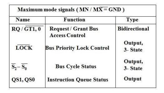
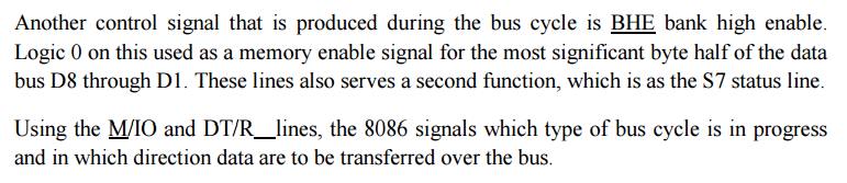
8288 Bus Controller – Bus Command and Control Signals: 8086 does not directly provide all the signals that are required to control the memory, I/O and interrupt interfaces. Specially the WR, M/IO, DT/R, DEN, ALE and INTA, signals are no longer produced by the 8086. Instead it outputs three status signals S0, S1, S2 prior to the initiation of each bus cycle. This 3- bit bus status code identifies which type of bus cycle is to follow. S2S1S0 are input to the external bus controller device, the bus controller generates the appropriately timed command and control signals.
The 8288 produces one or two of these eight command signals for each b us cycles. For instance, when the 8086 outputs the code S2S1S0 equals 001, it indicates that an I/O read cycle is to be performed. In the code 111 is output by the 8086, it is 75ignalling that no bus activity is to take place.
The control outputs produced by the 8288 are DEN, DT/R and ALE. These 3 signals provide the same functions as those described for the minimum system mode. This set of bus commands and control signals is compatible with the Multibus and industry standard for interfacing microprocessor systems.
8289 Bus Arbiter – Bus Arbitration and Lock Signals:
This device permits processors to reside on the system bus. It does this by implementing the Multibus arbitration protocol in an 8086-based system. Addition of the 8288 bus controller and 8289 bus arbiter frees a number of the 8086 pins for use to produce control signals that are needed to support multiple processors. Bus priority lock (LOCK) is one of these signals. It is input to the bus arbiter together with status signals S0 through S2.
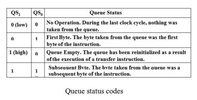
Queue Status Signals: Two new signals that are produced by the 8086 in the maximum-mode system are queue status outputs QS0 and QS1. Together they form a 2-bit queue status code, QS1QS0. Following table shows the four different queue status.
Related Topics