Chapter: Microprocessor and Microcontroller
Peripheral and Memory Mapped I/O Interfacing
PERIPHERAL MAPPED I/O INTERFACING
IN
instruction is used to access input device and OUT instruction is used to
access output device. Each I/O device is identified by a unique 8-bit address
assigned to it. Since the control signals used to access input and output
devices are different, and all I/O device use 8-bit address, a maximum of 256
(28) input devices and 256 output devices can be interfaced with
8085.
Ex:
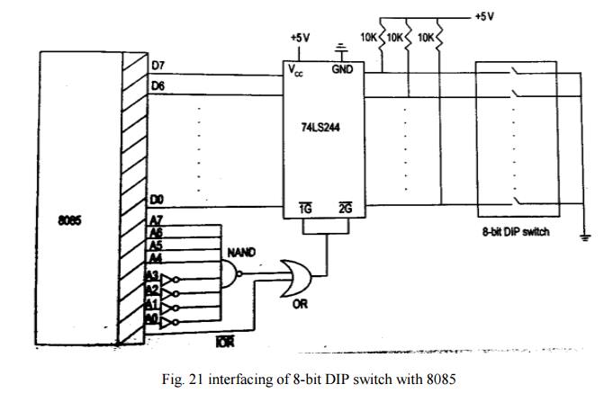
Interface an 8-bit DIP switch with the 8085 such that the address assigned to
the DIP switch if F0H.
IN
instruction is used to get data from DIP switch and store it in accumulator.
Steps involved in the execution of this instruction are:
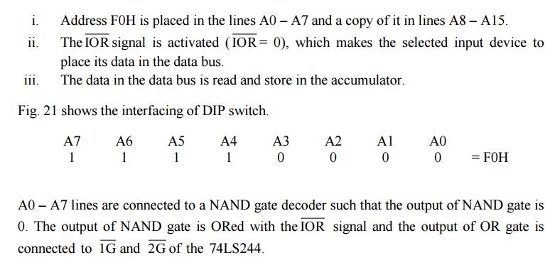
When
74LS244 is enabled, data from the DIP switch is placed on the data bus of the
8085. The 8085 read data and store in the accumulator. Thus data from DIP
switch is transferred to the accumulator.
MEMORY MAPPED I/O INTERFACING
In
memory-mapped I/O, each input or output device is treated as if it is a memory
location.
The
^(MEMR) and ^ (MEMW) control signals are used to activate the devices. Each
input or output device is identified by unique 16-bit address, similar to
16-bit address assigned to memory location. All memory related instruction like
LDA 2000H, LDAX B, MOV A, M can be used.
Since the
I/O devices use some of the memory address space of 8085, the maximum memory
capacity is lesser than 64 KB in this method.
Ex:
Interface an 8-bit DIP switch with the 8085 using logic gates such that the
address assigned to it is F0F0H.
Since a
16-bit address has to be assigned to a DIP switch, the memory-mapped I/O
technique must be used. Using LDA F0F0H instruction, the data from the 8-bit
DIP switch can be transferred to the
accumulator. The steps involved are:
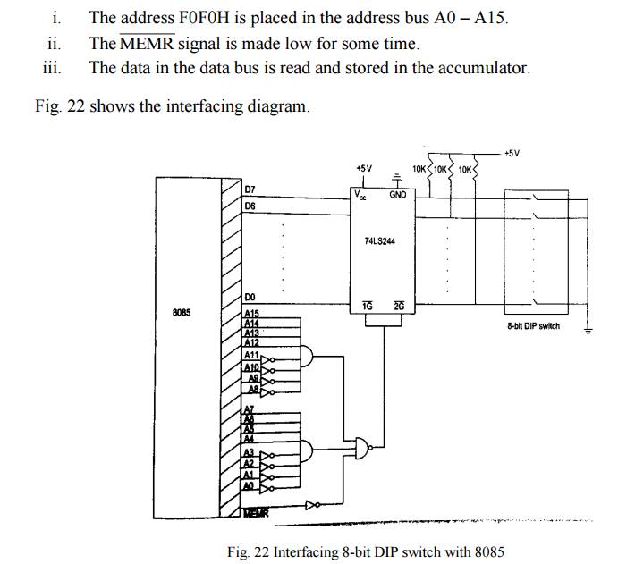
The address lines are connected to
AND gates. The output of these gates along with ^(MEMR) signal are connected to
a NAND gate, so that when the address F0F0H is placed in the address bus
and ^(MEMR) = 0 its output becomes 0,
thereby enabling the buffer 74LS244. The data from the DIP switch is placed in
the 8085 data bus. The 8085 reads the data from the data bus and stores it in
the accumulator.
Related Topics