Chapter: Microprocessor and Microcontroller
8085 Microprocessor Architecture
8085 MICROPROCESSOR ARCHITECTURE
The 8085
microprocessor is an 8-bit processor available as a 40-pin IC package and uses
+5 V for power. It can run at a maximum frequency of 3 MHz. Its data bus width
is 8-bit and address bus width is 16-bit, thus it can address 216 =
64 KB of memory. The internal architecture of 8085 is shown is Fig. 2.
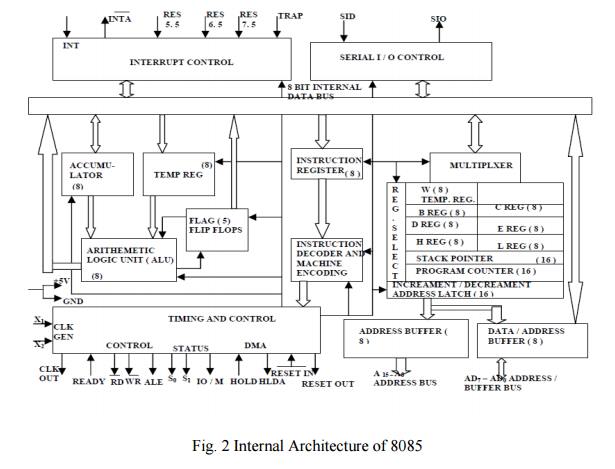
Arithmetic
and Logic Unit
The ALU
performs the actual numerical and logical operations such as Addition (ADD),
Subtraction (SUB), AND, OR etc. It uses data from memory and from Accumulator
to perform operations. The results of the arithmetic and logical operations are
stored in the accumulator.
Registers
The 8085
includes six registers, one accumulator and one flag register, as shown in Fig.
3. In addition, it has two 16-bit registers: stack pointer and program counter.
They are briefly described as follows.
The 8085
has six general-purpose registers to store 8-bit data; these are identified as
B, C, D, E, H and L. they can be combined as register pairs - BC, DE and HL to
perform some 16-bit operations. The programmer can use these registers to store
or copy data into the register by using data copy instructions.
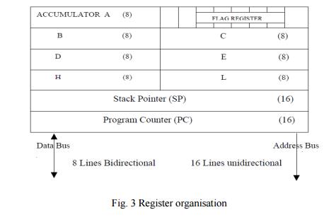
Accumulator
The
accumulator is an 8-bit register that is a part of ALU. This register is used
to store 8-bit data and to perform arithmetic and logical operations. The
result of an operation is stored in the accumulator. The accumulator is also
identified as register A.
Flag
register
The ALU
includes five flip-flops, which are set or reset after an operation according
to data condition of the result in the accumulator and other registers. They
are called Zero (Z), Carry (CY), Sign (S), Parity (P) and Auxiliary Carry (AC)
flags. Their bit positions in the flag register are shown in Fig. 4. The
microprocessor uses these flags to test data conditions.
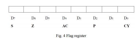
For
example, after an addition of two numbers, if the result in the accumulator is
larger than 8-bit, the flip-flop uses to indicate a carry by setting CY flag to
1. When an arithmetic operation results in zero, Z flag is set to 1. The S flag
is just a copy of the bit D7 of the accumulator. A negative number has a 1 in
bit D7 and a positive number has a 0 in 2’s complement representation. The AC
flag is set to 1, when a carry result from bit D3 and passes to bit D4. The P
flag is set to 1, when the result in accumulator contains even number of 1s.
Program
Counter (PC)
This
16-bit register deals with sequencing the execution of instructions. This
register is a memory pointer. The microprocessor uses this register to sequence
the execution of the instructions. The function of the program counter is to
point to the memory address from which the next byte is to be fetched. When a
byte is being fetched, the program counter is automatically incremented by one
to point to the next memory location.
Stack
Pointer (SP)
The stack
pointer is also a 16-bit register, used as a memory pointer. It points to a
memory location in R/W memory, called stack. The beginning of the stack is
defined by loading 16-bit address in the stack pointer.
Instruction
Register/Decoder
It is an
8-bit register that temporarily stores the current instruction of a program.
Latest instruction sent here from memory prior to execution. Decoder then takes
instruction and decodes or interprets the instruction. Decoded instruction then
passed to next stage.
Control
Unit
Generates
signals on data bus, address bus and control bus within microprocessor to carry
out the instruction, which has been decoded. Typical buses and their timing are
described as follows:
·
Data Bus: Data
bus carries data in binary form between microprocessor and other external units such as memory. It is
used to transmit data i.e. information, results of
arithmetic
etc between memory and the microprocessor. Data bus is bidirectional in nature.
The data bus width of 8085 microprocessor is 8-bit i.e. 28
combination of binary digits and are typically identified as D0 – D7. Thus size
of the data bus determines what arithmetic can be done. If only 8-bit wide then
largest number is 11111111 (255 in decimal). Therefore, larger numbers have to
be broken down into chunks of 255. This slows microprocessor.
·
Address
Bus: The
address bus carries addresses and is one way bus from microprocessor to the memory or other devices. 8085 microprocessor
contain 16-bit address bus and are generally identified as A0 - A15. The higher
order address lines (A8 – A15) are unidirectional and the lower order lines (A0
– A7) are multiplexed (time-shared) with the eight data bits (D0 – D7) and
hence, they are bidirectional.
·
Control
Bus: Control
bus are various lines which have specific functions for coordinating and controlling microprocessor operations. The
control bus carries control signals partly unidirectional and partly
bidirectional. The following control and status signals are used by 8085
processor:
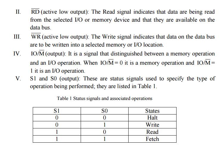
ALE (output): Address Latch Enable is a pulse that is provided when an
address appears on the AD0 – AD7 lines, after which it becomes 0.
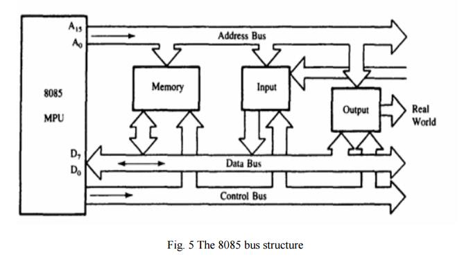
The
schematic representation of the 8085 bus structure is as shown in Fig. 5. The
microprocessor performs primarily four operations:
I.
Memory Read: Reads data (or instruction) from
memory.
II.Memory
Write: Writes data (or instruction) into memory.
III.I/O
Read: Accepts data from input device.
IV. I/O
Write: Sends data to output device.
The 8085 processor performs these functions using address bus, data bus
and control bus as shown in Fig. 5.
Related Topics