Chapter: Microprocessor and Microcontroller
Instruction Execution and Timing Diagram
INSTRUCTION EXECUTION AND TIMING DIAGRAM:
Each
instruction in 8085 microprocessor consists of two part- operation code
(opcode) and operand. The opcode is a command such as ADD and the operand is an
object to be operated on, such as a byte or the content of a register.
Instruction
Cycle: The time taken by the processor to complete the execution of an
instruction. An instruction cycle consists of one to six machine cycles.
Machine
Cycle: The time required to complete one operation; accessing either the memory
or I/O device. A machine cycle consists of three to six T-states.
T-State:
Time corresponding to one clock period. It is the basic unit to calculate
execution of instructions or programs in a processor.
To
execute a program, 8085 performs various operations as:
·
Opcode fetch
·
Operand fetch
·
Memory read/write
·
I/O read/write
External
communication functions are:
·
Memory read/write
·
I/O read/write
·
Interrupt request acknowledge
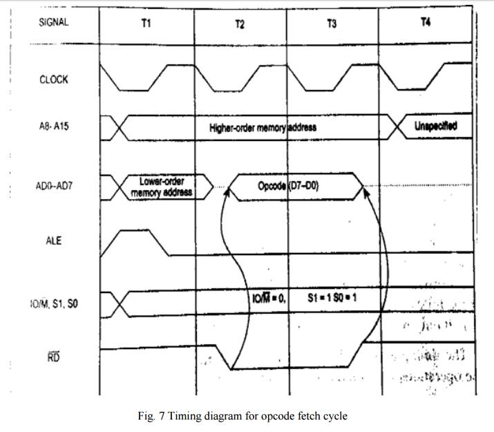
Opcode
Fetch Machine Cycle:
It is the
first step in the execution of any instruction. The timing diagram of this
cycle is given in Fig. 7.
The
following points explain the various operations that take place and the signals
that are changed during the execution of opcode fetch machine cycle:
T1 clock
cycle
i.
The content of PC is placed in the address bus; AD0
- AD7 lines contains lower bit address and A8 – A15 contains higher bit
address.
ii.
IO/^M signal is low indicating that a memory
location is being accessed. S1 and S0 also changed to the levels as indicated
in Table 1.
iii.
ALE is high, indicates that multiplexed AD0 – AD7
act as lower order bus.
T2 clock cycle
i. Multiplexed address bus is
now changed to data bus.
ii. The ^(RD) signal is made
low by the processor. This signal makes the memory device load the data bus
with the contents of the location addressed by the processor.
T3 clock cycle
i. The opcode available on the
data bus is read by the processor and moved to the instruction register.
ii. The ^(RD) signal is
deactivated by making it logic 1.
T4 clock cycle
i. The processor decode the
instruction in the instruction register and generate the necessary control
signals to execute the instruction. Based on the instruction further operations
such as fetching, writing into memory etc takes place.
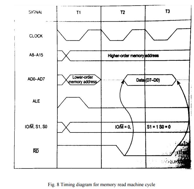
Memory
Read Machine Cycle:
The memory read cycle is executed by the processor to read a data byte
from memory. The machine cycle is exactly same to opcode fetch except: a) It
has three T-states b) The S0 signal is set to 0. The timing diagram of this
cycle is given in Fig. 8.
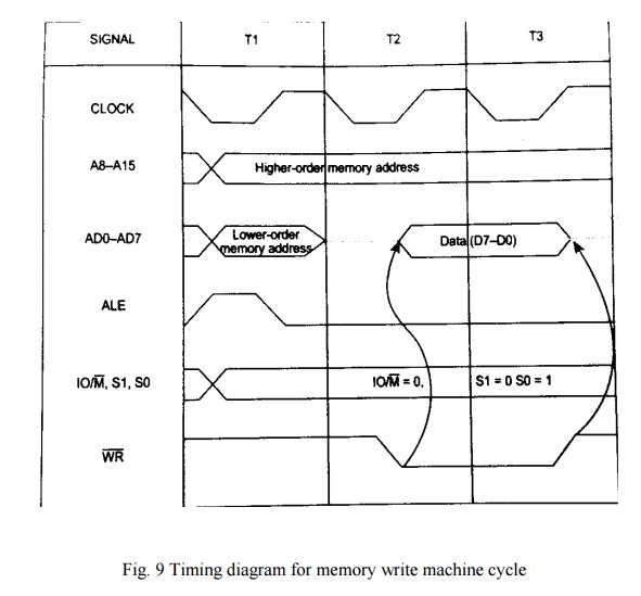
Memory Write Machine Cycle:
The memory write cycle is executed by the processor to write a data byte
in a memory location. The processor takes three T-states and ^(WR) signal is
made low. The timing diagram of this cycle is given in Fig. 9.
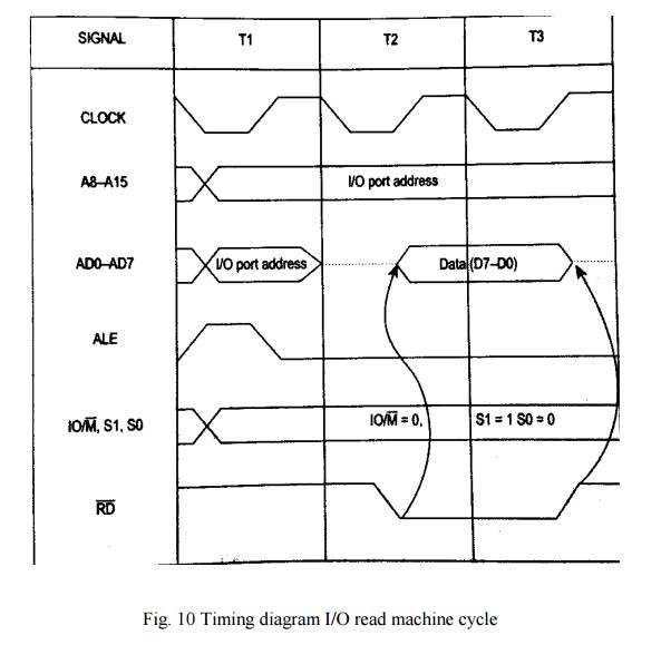
I/O Read Cycle:
The I/O read cycle is executed by the processor to read a data byte from
I/O port or from peripheral, which is I/O mapped in the system. The 8-bit port
address is placed both in the lower and higher order address bus. The processor
takes three T-states to execute this machine cycle. The timing diagram of this
cycle is given in Fig. 10.
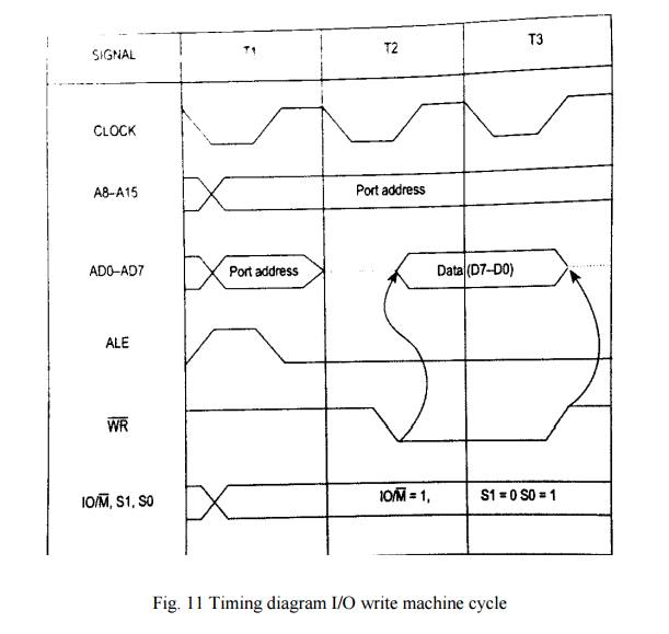
I/O Write
Cycle:
The I/O write cycle is executed by the processor to write a data byte to
I/O port or to a peripheral, which is I/O mapped in the system. The processor
takes three T-states to execute this machine cycle. The timing diagram of this
cycle is given in Fig. 11.
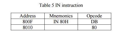
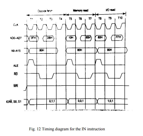
Ex:
Timing diagram for IN 80H.
The
instruction and the corresponding codes and memory locations are given in Table
5.
Table 5
IN instruction
i.
During the first machine cycle, the opcode DB is
fetched from the memory, placed in the instruction register and decoded.
ii.
During second machine cycle, the port address 80H
is read from the next memory location.
iii.
During the third machine cycle, the address 80H is
placed in the address bus and the data read from that port address is placed in
the accumulator.
The
timing diagram is shown in Fig. 12.
Related Topics