Chapter: Digital Logic Circuits : Asynchronous Sequential Circuits and Programmable Logic Devices
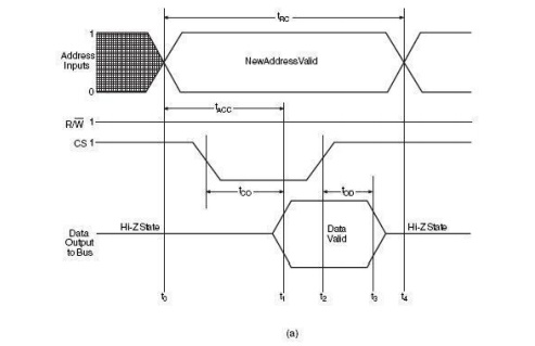
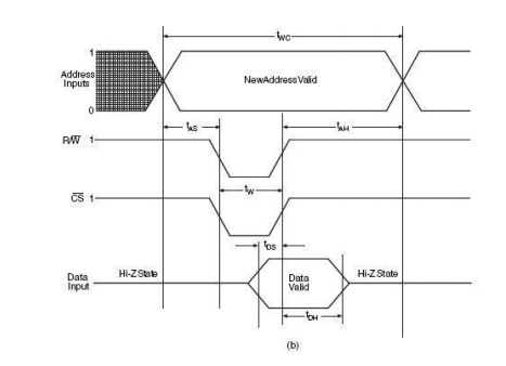
Random Access Memory
Random Access Memory
RAM has three basic building blocks, namely an array of memory cells arranged in rows and columns with each memory cell capable of storing either a ŌĆś0ŌĆś or a ŌĆś1ŌĆś, an address decoder and a read/write control logic. Depending upon the nature of the memory cell used, there are two types of RAM, namely static RAM (SRAM) and dynamic RAM (DRAM). In SRAM, the memory cell is essentially a latch and can store data indefinitely as long as the DC power is supplied. DRAM on the other hand, has a memory cell that stores data in the form of charge on a capacitor. Therefore, DRAM cannot retain data for long and hence needs to be refreshed periodically. SRAM has a higher speed of operation than DRAM but has a
smaller storage capacity.
Memory Expansion
When a given application requires a RAM or ROM with a capacity that is larger than what is available on a single chip, more than one such chip can be used to achieve the objective. The required enhancement in capacity could be either in terms of increasing the word size or increasing the number of memory locations.
Word Size Expansion
Let us take up the task of expanding the word size of an available 16├Ś 4 RAM chip from four bits to eight bits. Below figure shows a diagram where two such RAM chips have been used to achieve the desired effect. The arrangement is straightforward. Both chips are selected or deselected together. Also, the input that determines whether it is a ŌĆśreadŌĆś or ŌĆśwriteŌĆś operation is common to both chips. That is, both chips are selected for ŌĆśreadŌĆś or ŌĆśwriteŌĆśoperation together. The address inputs to the two chips are also common. The memory locations corresponding to various address inputs store four higher-order bits in the case of RAM-1 and four lower-order bits in the case of RAM-2. In essence, each of the RAM chips stores half of the word. Since the address inputs are common, the same location in each chip is accessed at the same time.
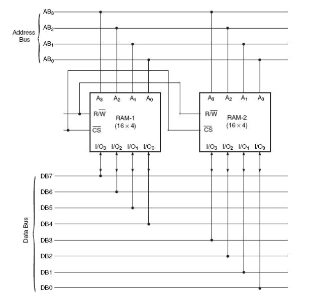
Word size expansion
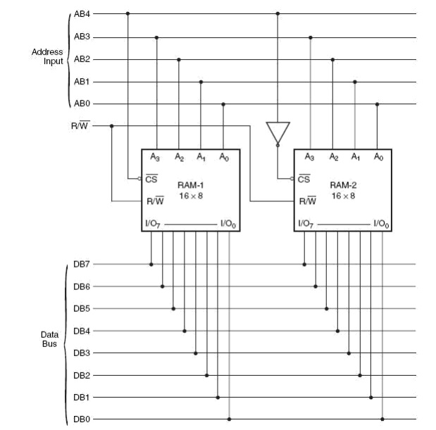
Memory Location Expansion
Below shows how more than one memory chip can be used to expand the number of memory locations. Let us consider the use of two 16├Ś 8 chips to get a 32├Ś 8 chip. A 32├Ś 8 chip would need five address input lines. Four of the five address inputs, other than the MSB address bit, are common to both 16├Ś 8 chips. The MSB bit feeds the input of one chip directly and the input of the other chip after inversion. The inputs to the two chips are common. Now, for first half of the memory locations corresponding to address inputs 00000 to 01111 (a total of 16 locations), the MSB bit of the address is ŌĆś0ŌĆś, with the result that RAM-1 is selected and RAM-2 is deselected. For the remaining address inputs of 10000 to 11111 (again, a total of 16 locations), RAM-1 is deselected while RAM-2 is selected. Thus, the overall arrangement offers a total of 32 locations, 16 provided by RAM-1 and 16 provided by RAM-2. The overall capacity is thus 32├Ś 8.
Related Topics