Chapter: Digital Logic Circuits : Asynchronous Sequential Circuits and Programmable Logic Devices
Programmable ROM
Programmable ROM
In the case of PROMs, instead of being done at
the manufacturer‘s premises during the manufacturing process, the
programming is done by the customer with the help of a special gadget called a
PROM programmer. Since the data, once programmed, cannot be erased and
reprogrammed, these devices are also referred to as one-time programmable ROMs.
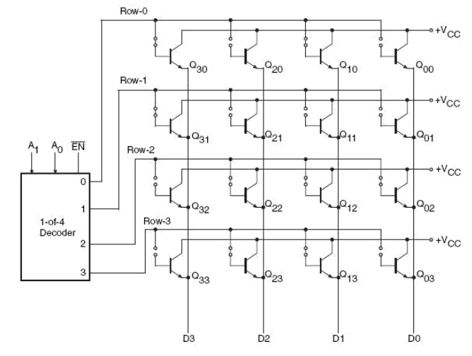
The basic memory cell of a PROM is similar to that of a mask-programmed ROM. Above
show a MOSFET-based memory cell and bipolar memory cell respectively. In the
case of a PROM, each of the connections that were left either intact or open in
the case of a mask-programmed ROM are made with a thin fusible link, as shown
in Fig. 15.18. The different interconnect technologies used in programmable
logic devices are comprehensively covered in Chapter 9. Basic fuse technologies
used in PROMs are metal links, silicon links and PN junctions. These fusible
links can be selectively blown off to store desired data. A sufficient current
is injected through the fusible link to burn it open to store ‘0‘. The programming operation, as said earlier, is done with a PROM
programmer. The PROM chip is plugged into the socket meant for the purpose. The
programmer circuitry selects each address of the PROM one by one, burns in the
required data and then verifies the correctness of the data before proceeding
to the next address. The data are fed to the programmer from a keyboard or a
disk drive or from a computer. PROM chips are available in various word sizes
and capacities. 27LS19, 27S21, 28L22, 27S15, 24S41, 27S35, 24S81, 27S45, 27S43
and 27S49 are respectively 32× 8, 256× 4, 256× 8, 512× 8, 1K× 4, 1K× 8, 2K× 4,
2K× 8, 4K× 8 and 8K× 8 PROMS. The typical access time in the case of these
devices is in the range 50–70 ns. MOS PROMs are available with much greater
capacities than bipolar PROMs. Also, the power dissipation is much lower in MOS
PROMs than it is in the case of bipolar PROMs with similar capacities


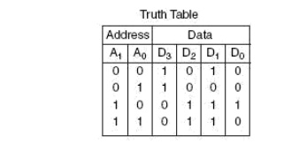
Internal structure of a 4 x 4 bipolar mask
programmed ROM

Related Topics