Chapter: Digital Logic Circuits : Asynchronous Sequential Circuits and Programmable Logic Devices
Mask programmed ROM
Mask-programmed ROM
In the case of a mask-programmed ROM, the ROM is
programmed at the manufacturer‘s site according to the specifications of the
customer. A photographic negative, called a mask, is used to store the required
data on the ROM chip. A different mask would be needed for storing each
different set
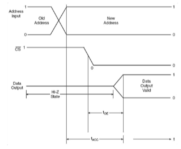
Typical timing diagram a ROM read operation of
information. As preparation of a mask is an expensive proposition,
mask-programmed ROM is economical only when manufactured in large quantities.
The limitation of such a ROM is that, once programmed, it cannot be
reprogrammed. The basic storage element is an NPN bipolar transistor, connected
in common-collector configuration, or a MOSFET in common drain configuration.
Figures 15.16(a) and (b) show a MOSFET-based basic cell connection when storing
a ‘1‘ and ‘0‘ respectively. As is clear from the figure, the
connection of the ‘row line‘ to the
gate of the MOSFET stores ‘1‘ at the location when the ‘row line‘ is set to level ‘1‘. A floating-gate connection is used to store ‘0‘. The data programmed into the ROM are given in the adjoining truth
table. The transistors with an open base store a ‘0‘, whereas
those with their bases connected to the corresponding decoder output store a ‘1‘. As an illustration, transistors Q30, Q20, Q10 and Q00 in row 0 store ‘1‘, ‘0‘, ‘1‘ and ‘0‘ respectively. The stored information in a given row is available at the
output when the corresponding decoder is enabled, and that ‘row line‘
is set to level ‘1‘. The
output of the memory cells appears at the column lines. For example, when the address input is ‘11‘, row 3 is
enabled and the data item at the output is 0110.
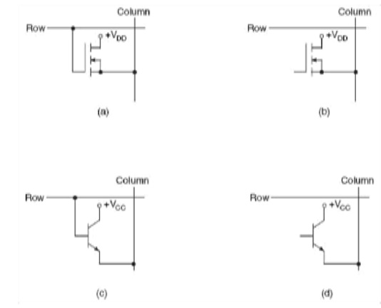
Basic cell connection of a mask programmed ROM
In the ROM architecture shown in Fig. 15.17, the
number of memory cells in a row represents the word size. The four memory cells
in a row here constitute a four-bit register. There are four such registers in
this ROM. In a 16× 8 ROM of this type there will be 16 rows of such transistor
cells, with each row having eight memory cells. The decoder in that case would
be a 1-of-16 decoder.
Related Topics