Chapter: Digital Electronics : Synchronous and Asynchronous Sequential Circuits
Concept of Sequential Logic
CONCEPT OF SEQUENTIAL LOGIC
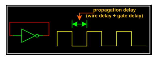
A sequential circuit as seen in the last page, is combinational logic with some feedback to maintain its current value, like a memory cell. To understand the basics let's consider the basic feedback logic circuit below, which is a simple NOT gate whose output is connected to its input. The effect is that output oscillates between HIGH and LOW (i.e. 1 and 0). Oscillation frequency depends on gate delay and wire delay. Assuming a wire delay of 0 and a gate delay of 10ns, then oscillation frequency would be (on time + off time = 20ns) 50Mhz.
The basic idea of having the feedback is to store the value or hold the value, but in the above circuit, output keeps toggling. We can overcome this problem with the circuit below, which is basically cascading two inverters, so that the feedback is in-phase, thus avoids toggling. The equivalent circuit is the same as having a buffer with its output connected to its input.
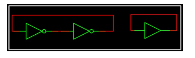
But there is a problem here too: each gate output value is stable, but what will it be? Or in other words buffer output can not be known. There is no way to tell. If we could know or set the value we would have a simple 1-bit storage/memory element.
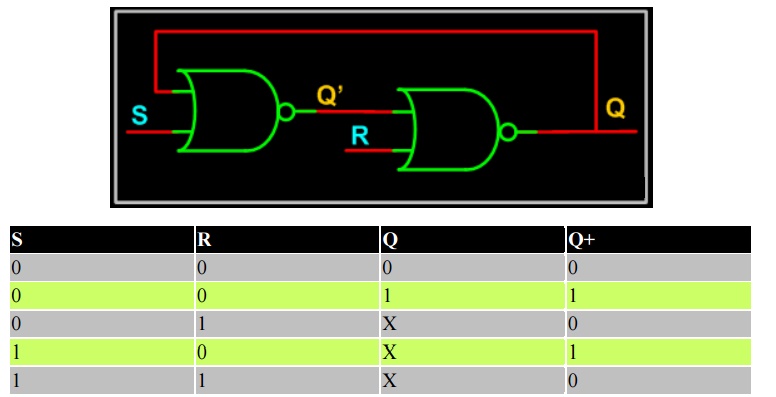
The circuit below is the same as the inverters connected back to back with provision to set the state of each gate (NOR gate with both inputs shorted is like a inverter). I am not going to explain the operation, as it is clear from the truth table. S is called set and R is called Reset.
There still seems to be some problem with the above configuration, we can not control when the input should be sampled, in other words there is no enable signal to control when the input is sampled. Normally input enable signals can be of two types.
· Level sensitive or (Latch)
· Edge Sensitive or (Flip-Flop)
1. Level Sensitive
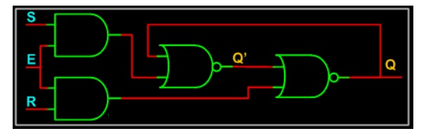
The circuit below is a modification of the above one to have level sensitive enable input. Enable, when LOW, masks the input S and R. When HIGH, presents S and R to the sequential logic input (the above circuit two NOR Gates). Thus Enable, when HIGH, transfers input S and R to the sequential cell transparently, so this kind of sequential circuits are called transparent Latch. The memory element we get is an RS Latch with active high Enable.
2. Edge Sensitive
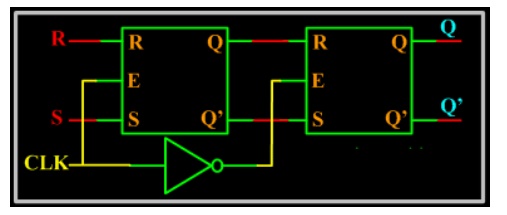
The circuit below is a cascade of two level sensitive memory elements, with a phase shift in the enable input between first memory element and second memory element. The first RS latch (i.e. the first memory element) will be enabled when CLK input is HIGH and the second RS latch will be enabled when CLK is LOW. The net effect is input RS is moved to Q and Q' when CLK changes state from HIGH to LOW, this HIGH to LOW transition is called falling edge. So the Edge Sensitive element we get is called negative edge RS flip-flop.
Now that we know the sequential circuits basics, let's look at each of them in detail in accordance to what is taught in colleges. You are always welcome to suggest if this can be written better in any way.
Related Topics