Chapter: Basic Electrical and electronics : Digital Electronics
Analog to Digital Conversion(ADC)
ANALOG TO DIGITAL CONVERSION
A
comparator compares the unknown voltage with a known value of voltage and then
produces proportional output (i.e. it will produce either a 1 or a 0). This
principle is basically used in the above circuit. Here three comparators are
used. Each has two inputs. One input of each comparator is connected to analog
input voltage. The other input terminals are connected to fixed reference
voltage like +3/4V, +V/2 and +V/4. Now the circuit can convert analog voltage
into equivalent digital signal. Since the analog output voltage is connected in
parallel to all the comparators, the circuit is also called as parallel A/D
converter.
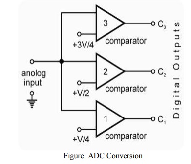
Working – Here each comparator is connected to
a reference voltage of +3/4V, +V/2 and +V/4
with their outputs as C3C2C1 respectively. Now
suppose the analog input voltage change from 0 – 4V, then the actual values of
reference voltages will be +3/4V = 3V, +V/2 =2V and +V/4 =1V. Now there will be
following conditions of outputs of the circuit
1) When input voltage is between 0 and 1V, the
output will be C3C2C1 = 000.
2) When input voltage > 1V £ 2V, the output
will be C3C2C1 = 001.
3) When input voltage > 2V £ 3V, the output
will be C3C2C1 = 011.
4) When input voltage > 3V £ 4V, the output
will be C3C2C1 = 111.
In this way, the circuit can convert the analog input voltage into
its equivalent or proportional binary number in digital style.
1 Successive Approximation Technique
The
basic drawback of counter method (given above) is that it has longer conversion
time. Because it always starts from 0000 at every measurement, until the analog
voltage is matched. This drawback is removed in successive approximation
method. In the adjacent figure, the method of successive approximation
technique is shown. When unknown voltage (Va) is applied, the
circuit starts up from 0000, as shown above. The output of SAR advances with
each MSB. The output of SAR does not increase step–by–step in BCD bus pattern,
but individual bit becomes high–starting from MSB. Then by comparison, the bit
is fixed or removed. Thus, it sets first MSB (1000), then the second MSB (0100)
and so on. Every time, the output of SAR is converted to equivalent analog
voltage by binary ladder. It is then compared with applied unknown voltage (Va).
The comparison process goes on, in binary search style, until the binary
equivalent of analog voltage is obtained. In this way following steps are
carried out during conversion.
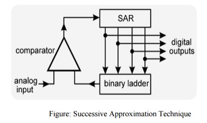
Figure: Successive Approximation Technique
Now
refer the following figure and the given steps -
1) The
unknown analog voltage (Va) is applied.
2) Starts up from 0000 and sets up first MSB 1000.
3) If Va >= 1000, the first MSB is
fixed.
4) If Va < 1000, the first MSB is
removed and second MSB is set
5) The fixing and removing the MSBs continues up
to last bit (LSB), until equivalent binary output is obtained.
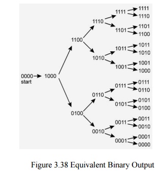
Figure 3.38 Equivalent Binary Output
2 Flash ADC
Also
called the parallel A/D converter, this circuit is the simplest to understand.
It is formed of a series of comparators, each one comparing the input signal to
a unique reference voltage. The comparator outputs connect to the inputs of a
priority encoder circuit, which then produces a binary output.
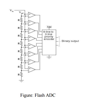
Figure:
Flash ADC
The
following illustration shows a 3-bit flash ADC circuit:
Vref is a stable reference voltage provided by a
precision voltage regulator as part of the converter circuit, not shown in the
schematic. As the analog input voltage exceeds the reference voltage at each comparator,
the comparator outputs will sequentially saturate to a high state. The priority
encoder generates a binary number based on the highest-order active input,
ignoring all other active inputs.
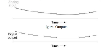
When
operated, the flash ADC produces an output that looks something like this
Related Topics