Chapter: Digital Logic Circuits : Asynchronous Sequential Circuits and Programmable Logic Devices
ROM Organization
ROM Organization
A circuit for implementing one or more switching
functions of several variables was described in the preceding section and
illustrated in Figure . The components of the circuit are
• An n × 2n decoder, with n input lines and 2n output
lines
• One or more OR gates, whose outputs are the circuit outputs
• An interconnection network between decoder outputs and
OR gate inputs
The decoder is an MSI circuit, consisting of 2n
n-input AND gates, that produces all the minterms of n variables. It achieves
some economy of implementation, because the same decoder can be used for any
application involving the same number of variables.What is special to any
application is the number of OR gates and the specific outputs of the decoder
that become inputs to those OR gates. Whatever else can be done to result in a
general-purpose circuit would be most welcome. The most general-purpose
approach is to include the maximum number of OR gates, with provision to
interconnect all 2n outputs of the decoder with the inputs to every one of the
OR gates. Then, for any given application, two things would have to be done:
•
The number
of OR gates used would be fewer than the maximum number, the others remaining
unused.
•
Not every
decoder output would be connected to all OR gate inputs.This scheme would be
terribly wasteful and doesn‘t sound like a good idea. Instead, suppose a
smaller number, m, is selected for the number of OR gates to be included, and
an interconnection network is set up to interconnect the 2n decoder outputs to
the m OR gate inputs. Such a structure is illustrated in Figure 21. It is an
LSI combinational circuit with n inputs and m outputs that, for reasons that
will become clear shortly, is called a read-only memory (ROM).
A ROM consists of two parts:
• An n × 2n decoder
•
A 2n × m
array of switching devices that form interconnections between the 2n lines from
the decoder and the m output lines The 2n output lines from the decoder are
called the word lines. Each of the 2n combinations that constitute the inputs
to the interconnection array corresponds to a minterm and specifies an
address.The memory consists of those connections that are actually made in the
connection matrix between the word lines and the output lines.
Once made, the connections in the memory array
are permanent.8 So this memory is not one whose contents can be changed readily
from time to time; we ―write‖ into this
memory but once. However, it is possible to ―read‖ the information already stored (the connections actually made) as often
as desired, by applying input words and observing the output words.That‘s why the circuit is called read-only memory. Before you continue
reading, think of two possible ways in which to fabricate a ROM so that one set
of connections can be made and another set left unconnected.
Continue reading after you have thought about
it.
A ROM can be almost completely fabricated except
that none of the connections are made. Such a ROM is said to be blank. Forming
the connections for a particular application is called programming the ROM. In
the process of programming the ROM, a mask is produced to cover those
connections that are not to be made. For this reason, the blank form of the ROM
is called mask programmable
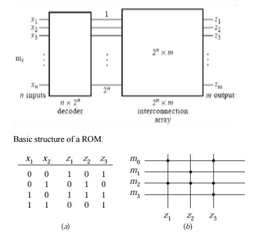
A ROM truth table and its program.
Related Topics