Chapter: Electrical and electronics : Circuit Theory : Transient Response For DC Circuits
Transient Response For DC Circuits
TRANSIENT RESPONSE FOR DC CIRCUITS
1. INTRODUCTION
2. TRANSIENT RESPONSE OF RL CIRCUITS
3. TRANSIENT RESPONSE OF RC CIRCUITS
4. TRANSIENT RESPONSE OF RLC CIRCUITS
5. CHARACTERIZATION OF TWO PORT NETWORKS IN TERMS OF Z,Y AND H PARAMETERS.
1. INTRODUCTION
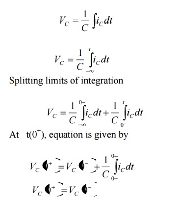
For higher order differential equation, the number of arbitrary constants equals the order of the equation. If these unknowns are to be evaluated for particular solution, other conditions in network must be known. A set of simultaneous equations must be formed containing general solution and some other equations to match number of unknown with equations.
We assume that at reference time t=0, network condition is changed by switching action. Assume that switch operates in zero time. The network conditions at this instant are called initial conditions in network.
1. Resistor :
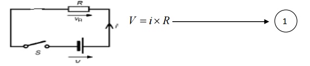
Equ 1 is linear and also time dependent. This indicates that current through resistor changes if applied voltage changes instantaneously. Thus in resistor, change in current is instantaneous as there is no storage of energy in it.
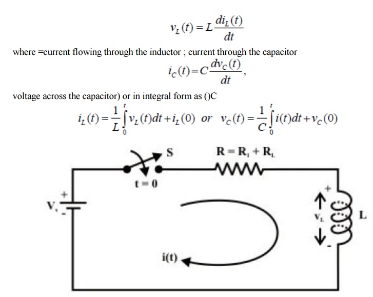
2.Inductor:
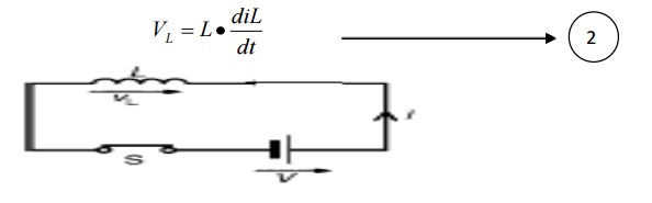
If dc current flows through inductor, dil/dt becomes zero as dc current is constant with respect to time. Hence voltage across inductor, VL becomes zero. Thus, as for as dc quantities are considered, in steady stake, inductor acts as short circuit.
We can express inductor current in terms of voltage developed across it as
I through inductor cannot change instantaneously.
3.capacitor
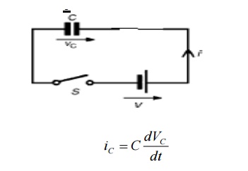
If dc voltage is applied to capacitor, dVC / dt becomes zero as dc voltage is constant with respect to time.
Hence the current through capacitor iC becomes zero, Thus as far as dc quantities are considered capacitor acts as open circuit.
Thus voltage across capacitor can not change instantaneously.
2. TRANSIENT RESPONSE OF RL CIRCUITS:
So far we have considered dc resistive network in which currents and voltages were independent of time. More specifically, Voltage (cause input) and current (effect output) responses displayed simultaneously except for a constant multiplicative factor (VR). Two basic passive elements namely, inductor and capacitor are introduced in the dc network. Automatically, the question will arise whether or not the methods developed in lesson-3 to lesson-8 for resistive circuit analysis are still valid. The voltage/current relationship for these two passive elements are defined by the derivative (voltage across the inductor
Our problem is to study the growth of current in the circuit through two stages, namely; (i) dc transient response (ii) steady state response of the system
D.C Transients: The behavior of the current and the voltage in the circuit switch is closed until it reaches its final value is called dc transient response of the concerned circuit. The response of a circuit (containing resistances, inductances, capacitors and switches) due to sudden application of voltage or current is called transient response. The most common instance of a transient response in a circuit occurs when a switch is turned on or off –a rather common event in an electric circuit.
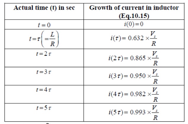
Growth or Rise of current in R-L circuit
To find the current expression (response) for the circuit shown in fig. 10.6(a), we can write the KVL equation around the circuit
The table shows how the current i(t) builds up in a R-L circuit.
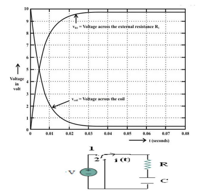
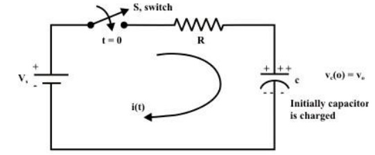
Consider network shown in fig. the switch k is moved from position 1 to 2 at reference time t = 0.
Now before switching take place, the capacitor C is fully charged to V volts and it discharges through resistance R. As time passes, charge and hence voltage across capacitor i.e. Vc decreases gradually and hence discharge current also decreases gradually from maximum to zero exponentially.
After switching has taken place, applying kirchoff’s voltage law,
Where VR is voltage across resistor and VC is voltage across capacitor.
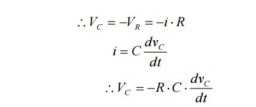
Above equation is linear, homogenous first order differential equation. Hence rearranging we have,
Integrating both sides of above equation we have
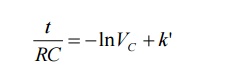
Now at t = 0, VC =V which is initial condition, substituting in equation we have,
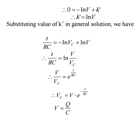
Where Q is total charge on capacitor
Similarly at any instant, VC = q/c where q is instantaneous charge.
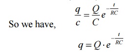
Thus charge behaves similarly to voltage across capacitor.
Now discharging current i is given by
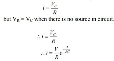
but VR = VC when there is no source in circuit.
The above expression is nothing but discharge current of capacitor. The variation of this current with respect to time is shown in fig.
For this network, after the instant t = 0, there is no driving voltage source in circuit, hence it is called undriven RC circuit.
3. TRANSIENT RESPONSE OF RC CIRCUITS
Ideal and real capacitors: An ideal capacitor has an infinite dielectric resistance and plates (made of metals) that have zero resistance. However, an ideal capacitor does not exist as all dielectrics have some
leakage current and all capacitor plates have some resistance. A capacitor’s of how much charge (current) it will allow to leak through the dielectric medium. Ideally, a charged
capacitor is not supposed to allow leaking any current through the dielectric medium and also assumed not to dissipate any power loss in capacitor plates resistance. Under this situation, the model as shown in fig. 10.16(a) represents the ideal capacitor. However, all real or practical capacitor leaks current to some extend due to leakage resistance of dielectric medium. This leakage resistance can be visualized as a resistance connected in parallel with the capacitor and power loss in capacitor plates can be realized with a resistance connected in series with capacitor. The model of a real capacitor is shown in fig.
Let us consider a simple series RC−circuit shown in fig. 10.17(a) is connected through a switch ‘S’ to a constant voltage source .
The switch ‘S’ is closed at time ‘t=0’ It is assumed that the capacitor is initially charged with a voltage and the current flowing through the circuit at any instant of time ‘’ after closing the switch is
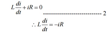
Current decay in source free series RL circuit: -
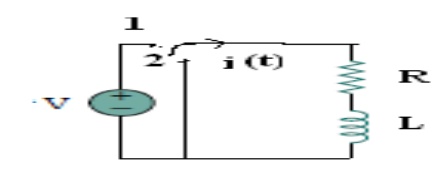
At t = 0- , , switch k is kept at position ‘a’ for very long time. Thus, the network is in steady state. Initial current through inductor is given as,
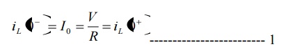
Because current through inductor can not change instantaneously
Assume that at t = 0 switch k is moved to position 'b'.
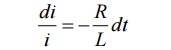
Applying KVL,
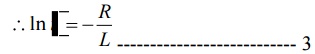
Rearranging the terms in above equation by separating variables
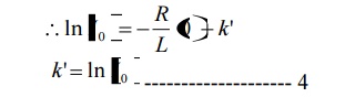
Integrating both sides with respect to corresponding variables
Where k’ is constant of integration.
To find- k’:
Form equation 1, at t=0, i=I0
Substituting the values in equation 3
Substituting value of k’ from equation 4 in
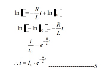
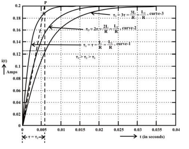
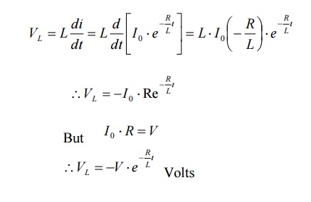
fig. shows variation of current i with respect to time
From the graph, H is clear that current is exponentially decaying. At point P on graph. The current value is (0.363) times its maximum value. The characteristics of decay are determined by values R and L which are two parameters of network.
The voltage across inductor is given by
4. TRANSIENT RESPONSE OF RLC CIRCUITS
In the preceding lesson, our discussion focused extensively on dc circuits having resistances with either inductor () or capacitor () (i.e., single storage element) but not both. Dynamic response of such first order system has been studied and discussed in detail. The presence of resistance, inductance, and capacitance in the dc circuit introduces at least a second order differential equation or by two simultaneous coupled linear first order differential equations. We shall see in next section that the complexity of analysis of second order circuits increases significantly when compared with that encountered with first order circuits. Initial conditions for the circuit variables and their derivatives play an important role and this is very crucial to analyze a second order dynamic system.
Response of a series R-L-C circuit
Consider a series RLcircuit as shown in fig.11.1, and it is excited with a dc voltage source C−−sV.
Applying around the closed path for ,
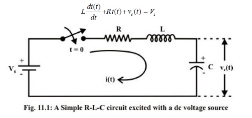
The current through the capacitor can be written as Substituting the current ‘’expression in eq.(11.1) and rearranging the terms,
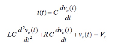
The above equation is a 2nd-order linear differential equation and the parameters associated with the differential equation are constant with time. The complete solution of the above differential equation has two components; the transient response and the steady state response. Mathematically, one can write the complete solution as
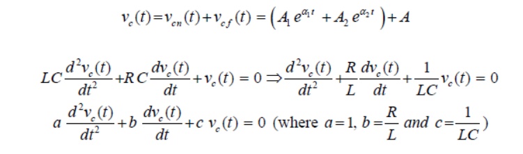
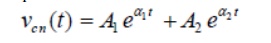
Since the system is linear, the nature of steady state response is same as that of forcing function (input voltage) and it is given by a constant value. Now, the first part of the total response is completely dies out with time while and it is defined as a transient or natural response of the system. The natural or transient response (see Appendix in Lesson-10) of second order differential equation can be obtained from the homogeneous equation (i.e., from force free system) that is expressed by

and solving the roots of this equation (11.5) on that associated with transient part of the complete solution (eq.11.3) and they are given below.

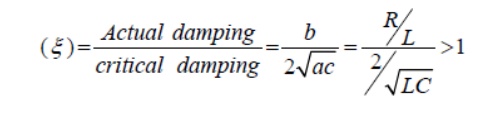
The roots of the characteristic equation are classified in three groups depending upon the values of the parameters ,,RLand of the circuit
Case-A (overdamped response): That the roots are distinct with negative real parts. Under this situation, the natural or transient part of the complete solution is written as
and each term of the above expression decays exponentially and ultimately reduces to zero as and it is termed as overdamped response of input free system. A system that is overdamped responds slowly to any change in excitation. It may be noted that the exponential term t→∞11tAeαtakes longer time to decay its value to zero than the term21tAeα. One can introduce a factorξ that provides an information about the speed of system response and it is defined by damping ratio
RLC Circuit:
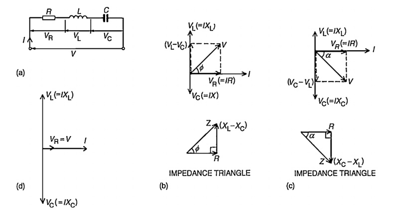
Consider a circuit in which R, L, and C are connected in series with each other across ac supply as shown in fig.
The ac supply is given by, V = Vm sin wt
The circuit draws a current I. Due to that different voltage drops are,
1. Voltage drop across Resistance R is VR = IR
2. Voltage drop across Inductance L is VL = IXL
3. Voltage drop across Capacitance C is Vc = IXc The characteristics of three drops are,
(i) VR is in phase with current I
(ii) VL leads I by 900
(iii) Vc lags I by 900
According to krichoff’s laws
Steps to draw phasor diagram:
1. Take current I as reference
2. VR is in phase with current I
3. VL leads current by 900
4. Vc lags current by 900
5. obtain resultant of VL and Vc. Both VL and Vc are in phase opposition (1800 out of phase)
6. Add that with VRby law of parallelogram to get supply voltage.
The phasor diagram depends on the condition of magnitude of VL and Vc which ultimately depends on values of XL and Xc.
Let us consider different cases:
Case(i): XL > Xc
When X L > Xc
Also VL > Vc (or) IXL > IXc
So, resultant of VL and Vc will directed towards VL i.e. leading current I. Hence I lags V i.e. current I will lags the resultant of VL and Vc i.e. (V L - Vc). The circuit is said to be inductive in nature.
From voltage triangle,
If , V = Vm Sin wt ; i = Im Sin (wt - ф )
i.e I lags V by angle ф
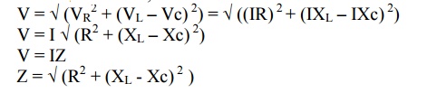
Case(ii): XL < Xc
When XL < Xc
Also VL < Vc (or) IXL < IXc
Hence the resultant of VL and Vc will directed towards Vc i.e current is said to be capacitive in nature
Form voltage triangle
i.e I lags V by angle ф
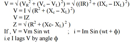
Case(iii): XL = Xc
When XL = Xc
Also VL = Vc (or) IXL = IXc
So VL and Vc cancel each other and the resultant is zero. So V = VR in such a case, the circuit is purely resistive in nature.
Impedance:
In general for RLC series circuit impedance is given by, Z = R + j X
X = XL –Xc = Total reactance of the circuit
If XL > Xc ; X is positive & circuit is Inductive
If XL < Xc ; X is negative & circuit is Capacitive
If XL = Xc ; X =0 & circuit is purely Resistive
Tan фL - =Xc[(X)∕R]
Cos ф = [R∕Z]
Z = 2 √+(X L(R-Xc ) 2)
Impedance triangle:
In both cases R = Z Cos ф
X = Z Sin ф
Power and power triangle:
The average power consumed by circuit is,
Pavg = (Average power consumed by R) + (Average power consumed by L) + (Average power consumed by C)
Pavg = Power taken by R = I2R = I(IR) = VI
V = V Cos ф P = VI Cos ф
Thus, for any condition, XL > Xc or XL < Xc General power can be expressed as
P = Voltage x Component in phase with voltage
Power triangle:
S = Apparent power = I2Z = VI
P = Real or True power = VI Cos ф = Active po Q = Reactive power = VI Sin ф
5. CHARACTERIZATION OF TWO PORT NETWORKS IN TERMS OF Z,Y AND H PARAMETERS.
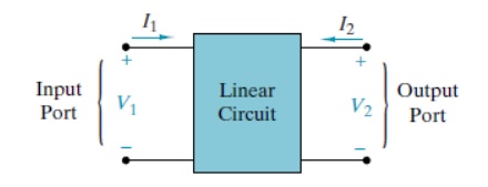
The purpose of this appendix is to study methods of characterizing and analyzing two-port networks. A port is a terminal pair where energy can be supplied or extracted. A two-port network is a four-terminal circuit in which the terminals are paired to form an input port and an output port. Figure W2–1 shows the customary way of defining the port voltages and currents. Note that the reference marks for the port variables comply with the passive sign convention.
The linear circuit connecting the two ports is
Assumed to be in the zero state and to be free of any independent sources. In other words, there is no initial energy stored in the circuit and the box in Figure W2–1 contains only resistors, capacitors, inductors, mutual inductance, and dependent sources. A four-terminal network qualifies as a two-port if the net current entering each terminal pair is zero. This means that the current exiting the lower port terminals in Figure W2–1 must be equal to the currents entering the upper terminals.
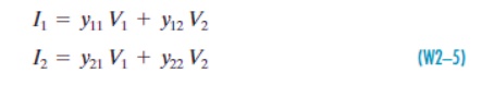
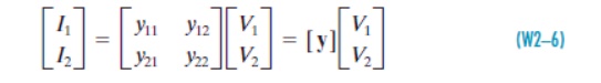
One way to meet this condition is to always connect external sources and loads between the input terminal pair or between the output terminal pair. The first task is to identify circuit parameters that characterize a two-port. In the two port approach the only available variables are the port voltages V1 and V2, and the port currents I1 and I2. A set of two-port parameters is defined by expressing two of these four-port variables in terms of the other two variables. In this appendix we study the four ways in Table W2–1.
TWO-PORT PARAMETERS
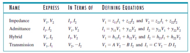
Note that each set of parameters is defined by two equations, one for each of the two dependent port variables. Each equation involves a sum of two terms, one for each of the two independent port variables. Each term involves a proportionality because the two-port is a linear circuit and superposition applies. The names given the parameters indicate their dimensions (impedance and admittance), a mixture of dimensions (hybrid), or their original application (transmission lines). With double-subscripted parameters, the first subscript indicates the port at which the dependent variable appears and the second subscript the port at which the independent variable appears.
Regardless of their dimensions, all two-port parameters are network functions. In general, the parameters are functions of the complex frequency variable and s-domain circuit analysis applies. For sinusoidalsteady-state problems, we replace s by j and use phasor circuit analysis. For purely resistive circuits, the two-port parameters are real constants and we use resistive circuit analysis. Before turning to specific parameters, it is important to specify the objectives of two-port network analysis. Briefly, these objectives are:
1. Determine two-port parameters of a given circuit.
Use two-port parameters to find port variable responses for specified input sources and output loads.
In principle, the port variable responses can be found by applying node or mesh analysis to the internal circuitry connecting the input and output ports. So why adopt the two-port point of view? Why not use straightforward circuit analysis?
There are several reasons. First, two-port parameters can be determined experimentally without resorting to circuit analysis. Second, there are applications in power systems and microwave circuits in which input and output ports are the only places that signals can be measured or observed. Finally, once two-port parameters of a circuit are known, it is relatively simple to find port variable responses for different input sources and/or different output loads.
put ports are the only places that signals can be measured or observed. Finally, once two-port parameters of a circuit are known, it is relatively simple to find port variable responses for different input sources and/or different output loads.
IMPEDANCE PARAMETERS
The impedance parameters are obtained by expressing the port voltages V1 and V2 in terms of the port currents I1 and I2.
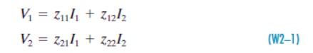
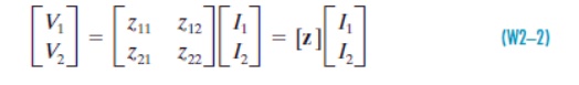
The network functions z11, z12, z21, and z22 are called the impedance parameters or simply the z-parameters. The matrix form of these equations are
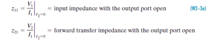
where the matrix [z] is called the impedance matrix of a two-port network. To measure or compute the impedance parameters, we apply excitation at one port and leave the other port open-circuited. When we drive port 1 with port 2 open (I2), the expressions in Eq. (W2–1) reduce to one term each, and yield the definitions of z11 and z21.
Conversely, when we drive port 2 with port 1 open (I1=0), the expressions in Eq. (W2–1) reduce to one term each that define z12and z22 as
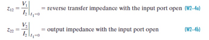
All of these parameters are impedances with dimensions of ohms. A two-port is said to be reciprocal when the open-circuit voltage measured at one port due to a current excitation at the other port is unchanged when the measurement and excitation ports are interchanged. A two-port that fails this test is said to be nonreciprocal. Circuits containing resistors, capacitors, and inductors (including mutual inductance) are always reciprocal. Adding dependent sources to the mix usually makes the two-port nonreciprocal. If a two-port is reciprocal, then z12 z21. To prove this we apply an excitation I1 Ix at the input port and observe that Eq. (W2–1) gives the open circuit (I2) voltage at the output port as V2OC z21Ix. Reversing the excitation and observation ports, we find that an excitation I2 Ix produces an open-circuit (I1) voltage at the input port of V 1OC z12Ix. Reciprocity requires that V1OC
V2OC, which can only happen if z12 z21.
ADMITTANCE PARAMETERS
The admittance parameters are obtained by expressing the port currents I1 and I2 in terms of the port voltages V1 and V2. The resulting two-port i–v relationships are
The network functions y11, y12, y21, and y22 are called the admittance parameters or simply the y-parameters. In matrix form these equations are
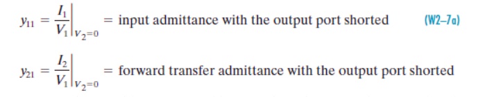
where the matrix [y ] is called the admittance matrix of a two-port network. To measure or compute the admittance parameters, we apply excitation at one port and short circuit the other port. When we drive at port 1 with port 2 shorted (V2= 0), the expressions in Eq. (W2–5) reduce to one term each that define y11 and y21 as
Conversely, when we drive at port 2 with port 1 shorted (V1= 0), the expressions in Eq. (W2– 5) reduce to one term each that define y22 and y12 as
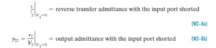
All of these network functions are admittances with dimensions of Siemens. If a two-port is reciprocal, then y12 y21. This can be proved using the same process applied to the z-parameters.
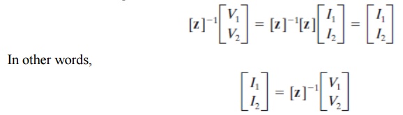
The admittance parameters express port currents in terms of port voltages, whereas the impedance parameters express the port voltages in terms of the port currents. In effect these parameters are inverses. To see this mathematically, we multiply Eq. (W2–2) by [z] 1, the inverse of the impedance matrix.
HYBRID PARAMETERS
The hybrid parameters are defined in terms of a mixture of port variables. Specifically, these parameters express V1 and I2 in terms of I1 and V2. The resulting two-port i–v relationships are
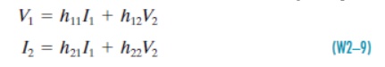
Where h11, h12, h21, and h22 are called the hybrid parameters or simply the h-parameters. In matrix form these equations are
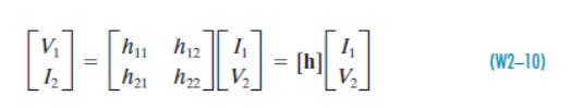
Where the matrix [h ] is called the h-matrix of a two-port network. The h-parameters can be measured or calculated as follows. When we drive at port 1 with port 2 shorted (V2= 0), the expressions in Eq. (W2–9) reduce to one term each, and yield the definitions of h11 and h21.
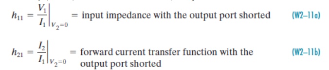
When we drive at port 2 with port 1 open (I1=0), the expressions in Eq. (W2–9) reduce to one term each, and yield the definitions of h12 and h22.
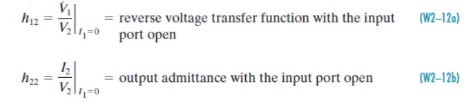
These network functions have a mixture of dimensions: h11 is impedance in ohms, h22 is admittance in Siemens, and h21 and h12 are dimensionless transfer functions. If a two-port is reciprocal, then h12h21. This can be proved by the same method applied to the z-parameters.
Related Topics