Chapter: Electrical and electronics : Circuit Theory : Transient Response For DC Circuits
Transient Response of RLC Circuits
TRANSIENT RESPONSE OF RLC CIRCUITS
In the preceding lesson, our discussion focused extensively on dc circuits having resistances with either inductor () or capacitor () (i.e., single storage element) but not both. Dynamic response of such first order system has been studied and discussed in detail. The presence of resistance, inductance, and capacitance in the dc circuit introduces at least a second order differential equation or by two simultaneous coupled linear first order differential equations. We shall see in next section that the complexity of analysis of second order circuits increases significantly when compared with that encountered with first order circuits. Initial conditions for the circuit variables and their derivatives play an important role and this is very crucial to analyze a second order dynamic system.
Response of a series R-L-C circuit
Consider a series RLcircuit as shown in fig.11.1, and it is excited with a dc voltage source C−−sV.
Applying around the closed path for ,
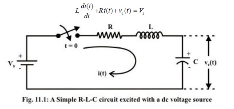
The current through the capacitor can be written as Substituting the current ‘’expression in eq.(11.1) and rearranging the terms,
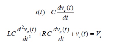
The above equation is a 2nd-order linear differential equation and the parameters associated with the differential equation are constant with time. The complete solution of the above differential equation has two components; the transient response and the steady state response. Mathematically, one can write the complete solution as
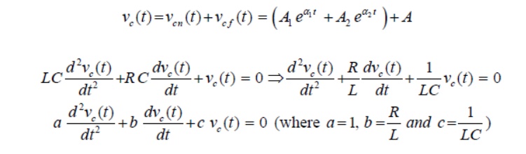
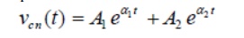
Since the system is linear, the nature of steady state response is same as that of forcing function (input voltage) and it is given by a constant value. Now, the first part of the total response is completely dies out with time while and it is defined as a transient or natural response of the system. The natural or transient response (see Appendix in Lesson-10) of second order differential equation can be obtained from the homogeneous equation (i.e., from force free system) that is expressed by

and solving the roots of this equation (11.5) on that associated with transient part of the complete solution (eq.11.3) and they are given below.

The roots of the characteristic equation are classified in three groups depending upon the values of the parameters ,,RLand of the circuit
Case-A (overdamped response): That the roots are distinct with negative real parts. Under this situation, the natural or transient part of the complete solution is written as
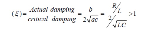
and each term of the above expression decays exponentially and ultimately reduces to zero as and it is termed as overdamped response of input free system. A system that is overdamped responds slowly to any change in excitation. It may be noted that the exponential term t→∞11tAeαtakes longer time to decay its value to zero than the term21tAeα. One can introduce a factorξ that provides an information about the speed of system response and it is defined by damping ratio
RLC Circuit:
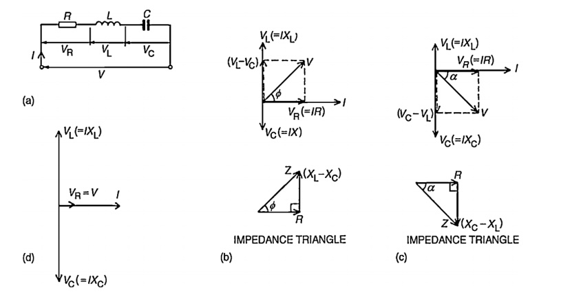
Consider a circuit in which R, L, and C are connected in series with each other across ac supply as shown in fig.
The ac supply is given by, V = Vm sin wt
The circuit draws a current I. Due to that different voltage drops are,
1. Voltage drop across Resistance R is VR = IR
2. Voltage drop across Inductance L is VL = IXL
3. Voltage drop across Capacitance C is Vc = IXc The characteristics of three drops are,
(i) VR is in phase with current I
(ii) VL leads I by 900
(iii) Vc lags I by 900
According to krichoff’s laws
Steps to draw phasor diagram:
1. Take current I as reference
2. VR is in phase with current I
3. VL leads current by 900
4. Vc lags current by 900
5. obtain resultant of VL and Vc. Both VL and Vc are in phase opposition (1800 out of phase)
6. Add that with VRby law of parallelogram to get supply voltage.
The phasor diagram depends on the condition of magnitude of VL and Vc which ultimately depends on values of XL and Xc.
Let us consider different cases:
Case(i): XL > Xc
When X L > Xc
Also VL > Vc (or) IXL > IXc
So, resultant of VL and Vc will directed towards VL i.e. leading current I. Hence I lags V i.e. current I will lags the resultant of VL and Vc i.e. (V L - Vc). The circuit is said to be inductive in nature.
From voltage triangle,
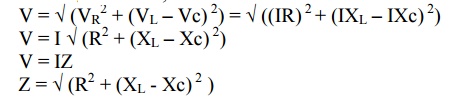
If , V = Vm Sin wt ; i = Im Sin (wt - ф )
i.e I lags V by angle ф
Case(ii): XL < Xc
When XL < Xc
Also VL < Vc (or) IXL < IXc
Hence the resultant of VL and Vc will directed towards Vc i.e current is said to be capacitive in nature
Form voltage triangle
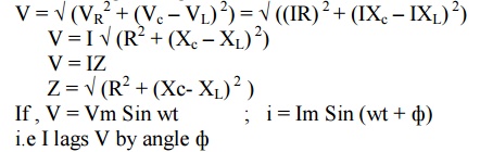
i.e I lags V by angle ф
Case(iii): XL = Xc
When XL = Xc
Also VL = Vc (or) IXL = IXc
So VL and Vc cancel each other and the resultant is zero. So V = VR in such a case, the circuit is purely resistive in nature.
Impedance:
In general for RLC series circuit impedance is given by, Z = R + j X
X = XL –Xc = Total reactance of the circuit
If XL > Xc ; X is positive & circuit is Inductive
If XL < Xc ; X is negative & circuit is Capacitive
If XL = Xc ; X =0 & circuit is purely Resistive
Tan фL - =Xc[(X)∕R]
Cos ф = [R∕Z]
Z = 2 √+(X L(R-Xc ) 2)
Impedance triangle:
In both cases R = Z Cos ф
X = Z Sin ф
Power and power triangle:
The average power consumed by circuit is,
Pavg = (Average power consumed by R) + (Average power consumed by L) + (Average power consumed by C)
Pavg = Power taken by R = I2R = I(IR) = VI
V = V Cos ф P = VI Cos ф
Thus, for any condition, XL > Xc or XL < Xc General power can be expressed as
P = Voltage x Component in phase with voltage
Power triangle:
S = Apparent power = I2Z = VI
P = Real or True power = VI Cos ф = Active po Q = Reactive power = VI Sin ф
Related Topics