Chapter: Electrical and electronics : Circuit Theory : Transient Response For DC Circuits
Phasor diagram for a series RLC circuit
Drawing of the phasor diagram for a series RLC
circuit energized by a sinusoidal voltage showing the relative position of
current, component voltage and applied voltage for the following case
a) When XL > Xc
c)
When XL = Xc.
RLC Circuit:
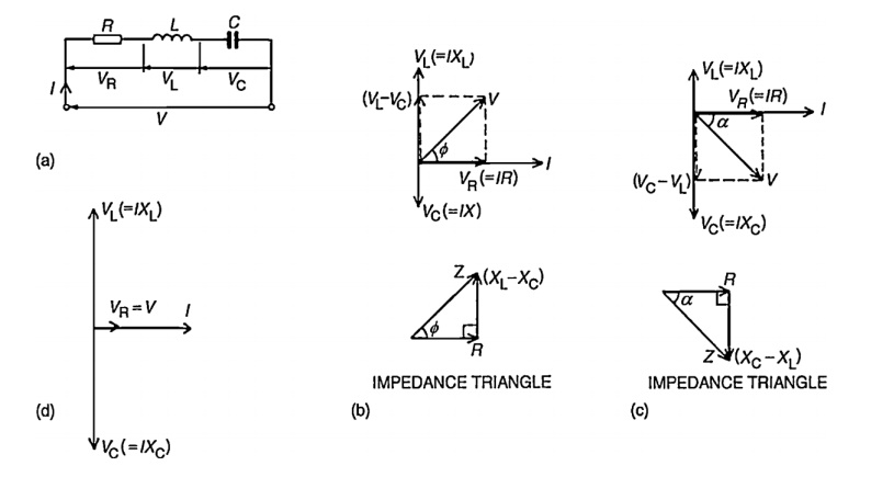
Consider a circuit in which R, L, and C are connected in series
with each other across ac supply as shown in fig.
The ac
supply is given by,
V = Vm sin wt
The
circuit draws a current I. Due to that different voltage drops are,
1) Voltage drop across Resistance R is VR
= IR
2) Voltage drop across Inductance L is VL
= IXL
3) Voltage drop across Capacitance C is Vc = IXc The
characteristics of three drops are,
1. VR is in phase with current I
2. VL leads I by 900
3. Vc lags I by 900
According
to krichoff’s laws
Steps to draw phasor diagram:
1. Take current I as reference
2. VR is in phase with current I
3. VL leads current by 900
4. Vc lags current by 900
5. obtain resultant of VL and Vc. Both
VL and Vc are in phase opposition (1800 out of phase)
6. Add that with VRby law of parallelogram to
getsupply voltage.
The phasor diagram depends on the condition of magnitude of VL
and Vc which ultimately depends on values of XL and Xc.
Let us
consider different cases:
Case(i): XL > Xc
When X L > Xc
Also VL
> Vc (or) IXL > IXc
So, resultant of VL and Vc will directed towards VL
i.e. leading current I. Hence I lags V i.e. current I will lags the resultant
of VL and Vc i.e. (VL - Vc). The circuit is said to be
inductive in nature.
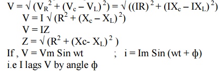
From
voltage triangle,
V = √ (VR2 + (VL
– Vc) 2) = √ ((IR) 2 + (IXL – IXc) 2)
V = I √ (R2 + (XL – Xc) 2)
V = IZ
Z = √ (R2 + (XL - Xc) 2
)
If , V = Vm Sin wt ; i = Im Sin (wt - ф)
i.e I
lags V by angle ф
Case(ii): XL < Xc
When XL
< Xc
Also VL
< Vc (or) IXL < IXc
Hence the resultant of VL and Vc will directed towards
Vc i.e current is said to be capacitive in nature Form voltage triangle
i.e I
lags V by angle ф
Case(iii): XL = Xc
When XL
= Xc
Also VL
= Vc (or) IXL = IXc
So VL and Vc cancel each other and the resultant is
zero. So V = VR in such a case, the circuit is purely resistive in
nature.
Impedance:
In general for RLC series circuit impedance is
given by,
Z = R + j X
X = XL – Xc = Total reactance of the
circuit
If XL > Xc ; X
is positive & circuit is Inductive
If XL < Xc ; X
is negative & circuit is Capacitive
If XL = Xc ; X =0 & circuit is purely Resistive
Tan ф = [(XL - Xc )∕R]
Cos ф = [R∕Z]
Z = √ (R2 + (XL - Xc ) 2)
Impedance
triangle:
In both cases R = Z Cos ф
X = Z Sin ф
Power
and power triangle:
The average power consumed by circuit is,
Pavg = (Average power consumed by R) + (Average
power consumed by L) + (Average power consumed by C)
Pavg = Power taken by R = I2R
= I(IR) = VI
V = V Cos ф
P = VI Cos ф
Thus, for any condition, XL > Xc
or XL < Xc General power can be expressed as
P = Voltage x Component in phase with voltage
Power
triangle:
S = Apparent power = I2Z = VI
P = Real or True power = VI Cos ф = Active
power
Q = Reactive power = VI Sin ф
Related Topics