Chapter: VLSI Design : CMOS Technology
Technology Related CAD Issues - CMOS Technology
TECHNOLOGY RELATED CAD ISSUES
Technology
CAD (or Technology Computer Aided Design, or TCAD) is a branch of electronic
design automation that models semiconductor fabrication and semiconductor
device operation.
The
modeling of the fabrication is termed Process TCAD, while the modeling of the
device operation is termed Device TCAD.
Included
are the modelling of process steps (such as diffusion and ion implantation),
and modelling of the behavior of the electrical devices based on fundamental
physics, such as the doping profiles of the devices.
TCAD may
also include the creation of compact models (such as the well known SPICE
transistor models), which try to capture the electrical behavior of such
devices but do not generally derive them from the underlying physics. (However,
the SPICE simulator itself is usually considered as part of ECAD rather than
TCAD.)
Today the
requirements for and use of TCAD cross-cut a very broad landscape of design
automation issues, including many fundamental physical limits.
At the
core are still a host of process and device modeling challenges that support
intrinsic device scaling and parasitic extraction.
These
applications include technology and design rule development, extraction of
compact models and more generally design for manufacturability (DFM).
The
dominance of interconnects for giga-scale integration (transistor counts in O
(billion)) and clocking frequencies in O (10 gigahertz)) have mandated the
development of tools and methodologies that embrace patterning by
electro-magnetic simulations both for optical patterns and electronic and
optical interconnect performance modeling as well as circuit-level modeling.
This
broad range of issues at the device and interconnect levels, including links to
underlying patterning and processing technologies, is summarized in Figure and
provides a conceptual framework for the discussion that now follows.
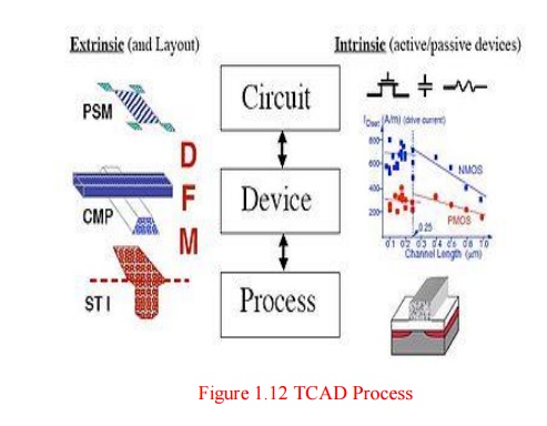
Figure :
Hierarchy of technology CAD tools building from the process level to circuits.
Left side icons show typical manufacturing issues; right side icons reflect MOS
scaling results based on TCAD (CRC Electronic Design Automation for IC
Handbook, Chapter 25)
Figure
depicts a hierarchy of process, device and circuit levels of simulation tools.
On each side of the boxes indicating modeling level are icons that
schematically depict representative applications for TCAD.
The left
side gives emphasis to Design For Manufacturing (DFM) issues such as:
shallow-trench isolation (STI), extra features required for phase-shift masking
(PSM) and challenges for multi-level interconnects that include processing
issues of chemical-mechanical planarization (CMP), and the need to consider
electro-magnetic effects using electromagnetic field solvers.
The right
side icons show the more traditional hierarchy of expected TCAD results and
applications: complete process simulations of the intrinsic devices,
predictions of drive current scaling and extraction of technology files for the
complete set of devices and parasitics.
Figure
again looks at TCAD capabilities but this time more in the context of design flow
information and how this relates to the physical layers and modeling of the
electronic design automation (EDA) world.
Here the
simulation levels of process and device modeling are considered as integral
capabilities (within TCAD) that together provide the "mapping" from
mask-level information to the functional capabilities needed at the EDA level
such as compact models ("technology files") and even higher-level
behavioral models.
Also
shown is the extraction and electrical rule checking (ERC); this indicates that
many of the details that to date have been embedded in analytical formulations,
may in fact also be linked to the deeper TCAD level in order to support the
growing complexity of technology scaling.
Related Topics