Chapter: VLSI Design : CMOS Technology
DC Transfer Characteristics of CMOS Inverter
DC TRANSFER CHARACTERISTICS OF
CMOS INVERTER
The general
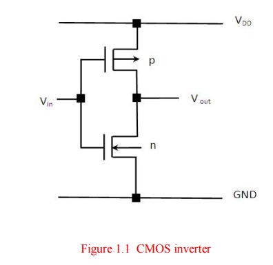
arrangement and characteristics are illustrated in Fig. 1 . 1 . The
current/voltage relationships for the MOS transistor may be written as,
Where Wn
and Ln, Wp and Lp are the n- and p- transistor
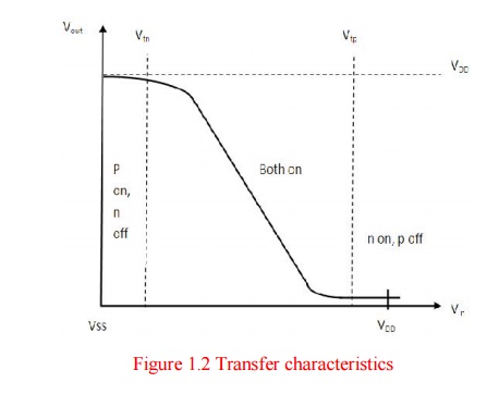
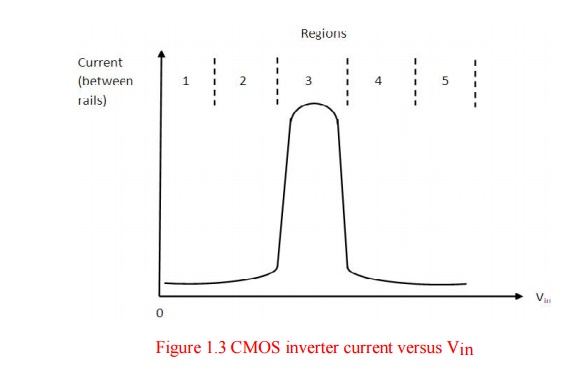
dimensions respectively. The CMOS inverter has five regions of operation is
shown in Fig.1.2 and in Fig. 1.3.
Considering
the static condition first, in region 1 for which Vin = logic 0, the
p-transistor fully turned on while the n-transistor is fully turned off. Thus
no current flows through the inverter and the output is directly connected to
VDD through the p-transistor.
In region
5 Vin = logic 1, the n-transistor is fully on while the p-transistor is fully
off. Again, no current flows and a good logic 0 appears at the output.
In region
2 the input voltage has increased to a level which just exceeds the threshold
voltage of the n-transistor. The n-transistor conducts and has a large voltage
between source and drain. The p- transistor also conducting but with only a
small voltage across it, it operates in the unsaturated resistive region
In region
4 is similar to region 2 but with the roles of the p- and n- transistors
reversed.
The
current magnitudes in region 2 and 4 are small and most of the energy consumed
in switching from one state to the other is due to the large current which
flows in region 3.
In region
3 is the region in which the inverter exhibits gain and in which both
transistors are in saturation.
Write
The
currents in each device must be the same since the transistors are in series.
So we may
I dsp = -
Idsn
Vin in
terms of the β ratio and the other circuit voltages and currents
Vin = VDD
+ Vtp +Vtn (βn + βp)1/2 / 1+ (βn + βp)1/2
Since
both transistors are in saturation, they act as current sources so that the
equivalent circuit in this region is two current sources so that the equivalent
circuit in this region is two current sources in series between VDD and VSS
with the output voltage coming from their common point.
The
region is inherently unstable in consequence and the change over from one logic
level to the other is rapid.
Since
only at this point will the two β factors be equal. But for βn= βp the device
geometries must be such that
µ pWp/Lp
= µ n Wn/Ln
The
motilities are inherently unequal and thus it is necessary for the width to
length ratio of the p- device to be three times that of the n-device, namely
Wp/Lp =
2.5 Wn/Ln
The
mobility µ is affected by the transverse electric field in the channel and is
thus independent onVgs.
It has
been shown empirically that the actual mobility is
µ= µ z (1 – Ø (Vgs – Vt)-1
Ø
is a constant approximately equal to 0.05 Vt
includes anybody effect, and µ z is the mobility with zero transverse field.
Related Topics