Chapter: Digital Logic Circuits : Combinational Circuits
Important Short Questions and Answers: Combinational Circuits
COMBINATIONAL CIRCUITS
1. Write
the procedural steps for the design of combinational circuits.
Solution
The design of combinational circuit
starts from a specification of the problem
culminates in a logic diagram or set
of Boolean equations from which the logic diagram can be obtained.
The procedure involves the following
steps:
1. From the specifications of the
circuit, determine the required number of inputs and outputs, and assign a
letter symbol to each.
2. Derive the truth table that defines
the required relation ship between inputs and
outputs.
3. Obtain the simplified Boolean
functions of each output as function of the input variables.
4. Draw the logic diagram.
5. Verify the correctness of the
design.
2.
Give the truth table for 4 bit priority encoder.
Solution:
A 4-bit priority encoder (also sometimes called a priority decoder). This
circuit basically converts the 4-bit input into a binary representation. If the
input n is active, all lower inputs (n-1…0) are ignored:
The circuit operation is simple.
Each output is driven by an OR-gate which is connected to the NAND-INV outputs
of the corresponding input lines. The NAND gate of each stages receives its
input bit, as well as the NAND gate outputs of all higher priority stages. This
structure implies that an active input on stage n effectively disables all
lower stages n-1.. 0.
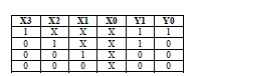
Note that the circuit function as
specified here does not depend at all on the least significant input bit.
A common use of priority encoders is
for interrupt controllers, to select the most critical out of multiple
interrupt requests. Due to electrical reasons (open collector outputs),
priority encoders with active-low inputs are also often used in practice.
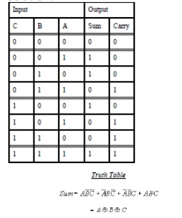
3.
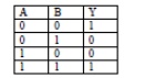
Draw the Truth Table of Full Adder.
Solution:
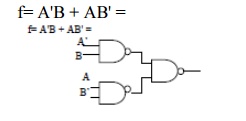
4.
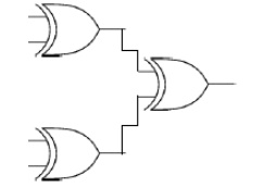
Realize f= A'B + AB' using minimum universal gates.
Solution:
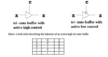
5.
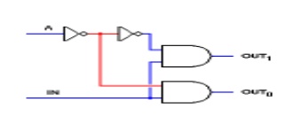
Draw a tristate inverter and draw its truth table .
Solution:
A tri-state buffer is a useful device that allows us to control when
current passes through the device, and when it doesn't. Here are two diagrams
of the tri-state buffer.
6.
Draw a combinational logic circuit which can compare whether two bit binary
numbers are same or not.
Solution:
Which is similar to EX-NOR operation
Y= A’B’+AB
7. What
is combinational circuit? Give an example.
Solution:
A combinational circuit consists of
logic gates whose outputs at any time are
determined from the present
combination of inputs. Examples of combinational circuits are adder, coder,
magnitude comparator etc.
8. What
are the universal gates?
Solution:
NAND and NOR are universal gates,
because they replace all the other gates in a circuit.
9. Obtain
3 level NOR – NOR implementation of f(a,b,c,d,e,f)=[ab+cd ]ef.
f (a, b, c, d, e, f)=[ab+cd ]ef
= abef +cdef
F’= (abef + cdef)’ =(abef)’.(cdef)’
= a+b+e+f . c+d+e+f
10.
Draw a 1 to 2-demultiplexer circuit.
Solution:
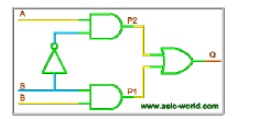
11.
Draw a 2 to 1 multiplexer circuit.
Solution
12.
What is demux?
Solution:
Demultiplexer is a circuit that
receives information on a single line and transmits this information on one of
2n possible output lines. A demultiplexer is a decoder with an enable input.
13.
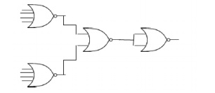
Draw a parity checker circuit for 3 bit binary word x1 x2 x3.
Solution:
14.
What does LS in 74LS00 indicate?
Solution:
Low power schottky TTL
15.
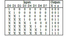
Define priority encoder.
Solution:
Encoders establish an input priority
to ensure that only the highest-priority input line is encoded. If priority is
given to an input with higher subscript number over one with lower subscript
number, then if both D2 and D5 are logic-1 simultaneously, the output will be
101 because D5 has a higher priority over D2.
Related Topics