Chapter: Linear Integrated Ciruits : Application of ICs
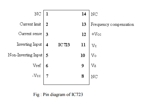
IC 723 - General Purpose Regulator
IC 723 - GENERAL PURPOSE
REGULATOR
Disadvantages
of fixed voltage regulator:
1.
Do not have the shot circuit protection
2.
Output voltage is not adjustable These limitations
can be overcomes in IC723.
Features
of IC723:
1.
Unregulated dc supply voltage at the input between
9.5V & 40V
2.
Adjustable regulated output voltage between 2 to
3V.
3.
Maximum load current of 150 mA (ILmax = 150mA).
4.
With the additional transistor used, ILmaxupto 10A
is obtainable.
5.
Positive or Negative supply operation
6.
Internal Power dissipation of 800mW.
7.
Built in short circuit protection.
8.
Very low temperature drift.
9.
High ripple rejection.
The
simplified functional block diagram can be divided in to 4 blocks.
1.
Reference generating block
2.
Error Amplifier
3.
Series Pass transistor
4.
Circuitry to limit the current
1.
Reference Generating block:
The
temperature compensated Zener diode, constant current source & voltage
reference amplifier together from the reference generating block. The Zener
diode is used to generate a fixed reference voltage internally. Constant
current source will make the Zener diode to operate at affixed point & it
is applied to the Non – inverting terminal of error amplifier. The Unregulated
input voltage ±Vcc is applied to the voltage reference amplifier as well as
error amplifier.
2. Error Amplifier:
Error
amplifier is a high gain differential amplifier with 2 input (inverting &
Non-inverting). The Non-inverting terminal is connected to the internally
generated reference voltage. The Inverting terminal is connected to the full
regulated output voltage.
3. Series Pass Transistor:
Q1
is the internal series pass transistor which is driven by the error amplifier.
This transistor actually acts as a variable resistor & regulates the output
voltage. The collector of transistor Q1 is connected to the
Un-regulated power supply. The maximum collector voltage of Q1 is
limited to 36Volts. The maximum current which can be supplied by Q1
is 150mA.
4. Circuitry to limit the current:
The
internal transistor Q2 is used for current sensing & limiting. Q2
is normally OFF transistor. It turns ON when the IL exceeds a predetermined
limit.
·
Low voltage, Low current is capable of supplying
load voltage which is equal to or between 2 to 7Volts.
Vload
= 2 to 7V
Iload
= 150mA
Related Topics