Chapter: VLSI Design : Specification Using Verilog HDL
Design Hierarchies - VLSI Design
DESIGN HIERARCHIES
1. CMOS Gates
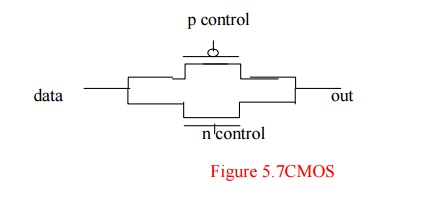
The cmos
gate is the combination of a pmos gate and an nmos gate. The rcmos (resistive
cmos) gate is the combination of an rpmos gate and an rnmos gate. The combined
gates in these configurations share data input and data output terminals, but
they have separate control inputs.
2. Cmos switch:
Declarations
of these gates begin with one of these keywords:
·
CMOS
·
RCMOS
The delay
specification can be 0, 1, 2 or 3 delays. If there is no delay, there is no
delay through the gate. A single delay specifies the delay for all transitions.
If the
specification contains two delays, the first delay determines the rise delay,
the second delay determines the fall delay, and the smaller of the two delays
is the delay of transitions to Zand X.
If the
specification contains three delays, the first delay controls rise delays, the
second delay controls fall delays, the third delay controls transitions to Z,
and the smallest of the three delays applies to transitions to X. Delays in
transitions to H or L are the same as delays in transitions to X.
The cmos
and rcmos gates have a data input, a data output and 2 control inputs. In the
terminal list, the first terminal connects to the data output, the second
connects to the data input, the third connects to the n-channel control input
and the last connects to the p-channel control input.
The
equivalence of the cmos gate to the pairing of an nmos gate and a pmos gate is
detailed in the following explanation:
cmos (w,
datain, ncontrol, pcontrol);
is
equivalent to:
nmos (w,
datain, ncontrol);
pmos (w,
datain, pcontrol);
3. pullup and pulldown
Sources
Declarations
of these sources begin with one of the following keywords:
pulluppulldown
A
strength specification follows the keyword and an optional identifier follows
the strength specification. A terminal list completes the declaration.
A pullup
source places a logic value of one on the nets listed in its terminal list. A
pulldown source places a logic value of zero on the nets listed in its terminal
list. The signals that these sources place on nets have pull strength in the
absence of a strength specification. There are no delay specifications for
these sources because the signals they place on nets continue throughout
simulation without variation.
The
following example declares two pullup instances:
pullup
(strong1, strong0)(neta),(netb);
In this
example, one gate instance drives neta, the other drives netb.
Related Topics