Chapter: Basic Electrical and Electronics Engineering
BJT
BJT
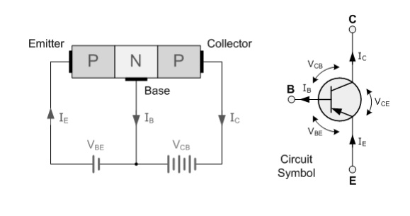
A bipolar junction transistor (BJT) is a three-terminal electronic device constructed of doped semiconductor material.
It may be used in amplifying or switching applications.
Bipolar transistors are so named because their operation involves both electrons and holes.
Charge flow in a BJT is due to bidirectional diffusion of charge carriers across a junction between two regions of different charge concentrations.
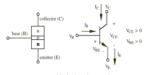
3 adjacent regions of doped Si (each connected to a lead):
o Base. (thin layer,less doped).
o Collector.
o Emitter.
2 types of BJT:
o npn.
o pnp.
npn bipolar junction transistor:
npn bipolar junction transistor
• 1 thin layer of p-type, sandwiched between 2 layers of n-type.
• N-type of emitter: more heavily doped than collector.
• With VC>VB>VE:
– Base-Emitter junction forward biased, Base-Collector reverse biased.
– Electrons diffuse from Emitter to Base (from n to p).
– There‘s a depletion layer on the Base-Collector junction -- -- > no flow of e- allowed.
– BUT the Base is thin and Emitter region is n+ (heavily doped) -- -- > electrons have enough momentum to cross the Base into the Collector.
– The small base current IB controls a large current IC
pnp bipolar junction transistor:
pnp bipolar junction transistor
• 1 thin layer of n-type, sandwiched between 2 layers of p-type.
• P-type of emitter: more heavily doped than collector.
• The voltages vEB and vCB are positive when they forward bias their respective pn junctions.
• Collector current and base current exit the transistor terminals and emitter current enters the device.
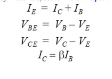
• Base current is given by:
Emitter current is given by:
Operation of NPN and NPN Transistor
Operation of NPN Transistor:
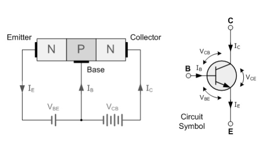
Forward-biased junction:
With the emitter-to-base junction in the figure biased in the forward direction, electrons leave the negative terminal of the battery and enter the n- material (emitter).
Since electrons are majority current carriers in the n- material, they pass easily through the emitter, cross over the junction, and combine with holes in the p material (base).
For each electron that fills a hole in the p material, another electron will leave the p material (creating a new hole) and enter the positive terminal of the battery.
Reverse-biased junction:
The second pn- junction (base-to-collector), or reverse-biased junction as it is called blocks the majority current carriers from crossing the junction.
However, there is a very small current, that does pass through this junction.
This current is called minority current, or reverse current. This current was produced by the electron-hole pairs.
The minority carriers for the reverse-biased pn- junction are the electrons in the p material and the holes in the n- material.
These minority carriers actually conduct the current for the reverse-biased junction when electrons from the p material enter the n material, and the holes from the n- material enter the p- material.
However, the minority current electrons play the most important part in the operation of the npn transistor.
Total current flow in the npn transistor is through the emitter lead. Therefore, in terms of percentage, IE is 100 percent.
On the other hand, since the base is very thin and lightly doped, a smaller percentage of the total current (emitter current) will flow in the base circuit than in the collector circuit.
Usually no more than 2 to 5 percent of the total current is base current (IB) while the remaining 95 to 98 percent is collector current (IC).
A very basic relationship exists between these two currents:
IE = IB + IC
Operation of PNP Transistor:
Forward Biased Junction:
With the bias setup shown, the positive terminal of the battery repels the emitter holes toward the base, while the negative terminal drives the base electrons toward the emitter.
When an emitter hole and a base electron meet, they combine.
For each electron that combines with a hole, another electron leaves the negative terminal of the battery, and enters the base.
At the same time, an electron leaves the emitter, creating a new hole, and enters the positive terminal of the battery.
This movement of electrons into the base and out of the emitter constitutes base current flow (IB), and the path these electrons take is referred to as the emitter-base circuit.
Reverse Biased Junction:
In the reverse-biased junction the negative voltage on the collector and the positive voltage on the base block the majority current carriers from crossing the junction.
However, this same negative collector voltage acts as forward bias for the minority current holes in the base, which cross the junction and enter the collector.
The minority current electrons in the collector also sense forward bias-the positive base voltage-and move into the base.
The holes in the collector are filled by electrons that flow from the negative terminal of the battery.
At the same time the electrons leave the negative terminal of the battery, other electrons in the base break their covalent bonds and enter the positive terminal of the battery.
Although there is only minority current flow in the reverse-biased junction, it is still very small because of the limited number of minority current carriers.
Related Topics