Chapter: Basic Electrical and Electronics Engineering : Digital Electronics
Shift Registers
Shift Registers
Shift Registers consists
of a number of single bit "D-Type Data Latches" connected together in a chain arrangement so that the output from
one data latch becomes the input of the next latch and so on, thereby moving
the stored data serially from either the left or the right direction. The
number of individual Data Latches used to make up Shift Registers are determined by the number of bits to be stored
with the most common being 8-bits wide. Shift Registers are mainly used to
store data and to convert data from either a serial to parallel or parallel to
serial format with all the latches being driven by a common clock (Clk) signal
making them Synchronous devices. They are generally provided with a Clear or Reset
connection so that they can be "SET" or "RESET" as
required.
Generally,
Shift Registers operate in one of four different modes:
Serial-in
to Parallel-out (SIPO)
![]()
Serial-in
to Serial-out (SISO)
![]()
Parallel-in
to Parallel-out (PIPO)
![]()
Parallel-in
to Serial-out (PISO)
![]()
Serial-in to Parallel-out.
4-bit Serial-in to Parallel-out
(SIPO) Shift Register
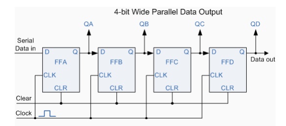
Lets
assume that all the flip-flops (FFA to FFD) have just been RESET (CLEAR input)
and that all the outputs QA to QD are at logic level "0" ie, no
parallel data output. If a logic "1" is connected to the DATA input
pin of FFA then on the first clock pulse the output of FFA and the resulting QA
will be set HIGH to logic "1" with all the other outputs remaining
LOW at logic "0". Assume now that the DATA input pin of FFA has
returned LOW to logic "0". The next clock pulse will change the
output of FFA to logic "0" and the output of FFB and QB HIGH to logic
"1". The logic "1" has now moved or been
"Shifted" one place along the register to the right. When the third
clock pulse arrives this logic "1" value moves to the output of FFC
(QC) and so on until the arrival of the fifth clock pulse which sets all the
outputs QA to QD back again to logic level "0" because the input has
remained at a constant logic level "0".
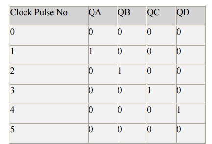
The
effect of each clock pulse is to shift the DATA contents of each stage one
place to the right, and this is shown in the following table until the complete
DATA is stored, which can now be read directly from the outputs of QA to QD.
Then the
DATA has been converted from a Serial Data signal to a Parallel Data word.
![]()
![]()
![]() Serial-in to Serial-out
Serial-in to Serial-out
This
Shift Register is very similar to the one above except where as the data was
read directly in a parallel form from the outputs QA to QD, this time the DATA
is allowed to flow straight through the register. Since there is only one
output the DATA leaves the shift register one bit at a time in a serial pattern
and hence the name Serial-in to
Serial-Out Shift Register.
4-bit Serial-in to Serial-out
(SISO) Shift Register

This type
of Shift Register also acts as a
temporary storage device or as a time delay device, with the amount of time
delay being controlled by the number of stages in the register, 4, 8, 16 etc or
by varying the application of the clock pulses. Commonly available IC's include
the 74HC595 8-bit Serial-in/Serial-out Shift Register with 3-state outputs.
Parallel-in to Serial-out
Parallel-in
to Serial-out Shift Registers act in the opposite way to the Serial-in to
Parallel-out one above. The DATA is applied in parallel form to the parallel
input pins PA to PD of the register and is then read out sequentially from the
register one bit at a time from PA to PD on each clock cycle in a serial
format.
4-bit Parallel-in to Serial-out
(PISO) Shift Register
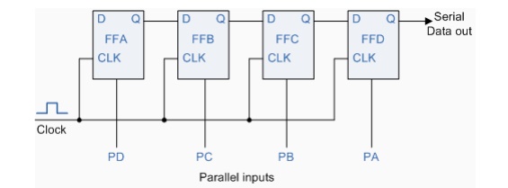
As this
type of Shift Register converts parallel data, such as an 8-bit data word into
serial data it can be used to multiplex many different input lines into a
single serial DATA stream which can be sent directly to a computer or
transmitted over a communications line. Commonly available IC's include the
74HC165 8-bit Parallel-in/Serial-out Shift Registers.
Parallel-in to Parallel-out
Parallel-in
to Parallel-out Shift Registers also act as a temporary storage device or as a
time delay device. The DATA is presented in a parallel format to the parallel
input pins PA to PD and then shifts it to the corresponding output pins QA to
QD when the registers are clocked.
4-bit Parallel-in/Parallel-out
(PIPO) Shift Register
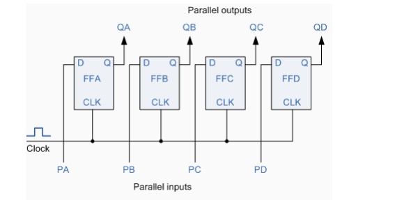
As with
the Serial-in to Serial-out shift register, this type of register also acts as
a temporary storage device or as a time delay device, with the amount of time
delay being varied by the frequency of the clock pulses.
Today,
high speed bi-directional universal type Shift
Registers such as the TTL 74LS194, 74LS195 or the CMOS 4035 are available
as a 4-bit multi-function devices that can be used in serial-serial, shift
left, shift right, serial-parallel, parallel-serial, and as a parallel-parallel
Data Registers, hence the name "Universal".
Ring Counters
we apply
a serial data signal to the input of a Serial-in to Serial-out Shift Register,
the same sequence of data will exit from the last flip-flip in the register
chain after a preset number of clock cycles thereby acting as a time delay to
the original signal. But what if we were to connect the output of the Shift
Register back to its input, we then have a closed loop circuit that "Recirculates"
the DATA around a loop, and this is the principal operation of
Ring Counters or Walking Ring Counter. Consider the circuit below.
4-bit Ring Counter

The
synchronous Ring Counter example
above, will re-circulate the same DATA pattern between the 4 Flip-flops over
and over again every 4th clock cycle, as long as the clock pulses are applied
to it. But in order to cycle the DATA we must first "Load" the
counter with a suitable DATA pattern for it to work correctly as all logic
"0"'s or all logic "1"'s outputted at each clock cycle
would make the ring counter invalid.
For Ring Counters to operate correctly they
must start with the first flip-flop (FFA) in the logic "1" state and
all the others at logic "0". To achieve this, a "CLEAR"
signal is firstly applied to all the Flip-flops in order to "RESET"
their outputs to a logic "0" level and then a "PRESET"
pulse is applied to the input of the first Flip-flop (FFA) before the clock pulses
are applied. This then places a single logic "1" value into the
circuit of the Ring Counters.
The ring
counter example shown above is also known as a "MODULO-4" or "MOD-4" counter since it has 4 distinct
stages and each Flip-flop output has a frequency equal to one-fourth or a
quarter (1/4) that of the main clock frequency. The "MODULO" or
"MODULUS" of a counter is the number of states the counter counts or
sequences through before repeating itself and a ring counter can be made to
output any MODULO number and a "MOD-N" Ring Counter will require
"N" number of Flip-flops connected together. For example, a MOD-8
Ring Counter requires 8 Flip-flops and a MOD-16 Ring Counter would require 16
Flip-flops.
Johnson Ring Counters
Johnson Ring Counters or
"Twisted Ring Counters", are exactly the same idea as the Walking Ring Counter above, except that the inverted output Q of
the last Flip-flop is connected back to the input D of the first Flip-flop as
shown below. The main advantage of this type of ring counter is that it only
needs half the number of Flip-flops compared to the standard walking ring
counter then its Modulo number is halved.
4-bit Johnson Ring Counter
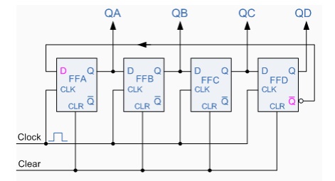
This
inversion of Q before it is fed back to input D causes the counter to
"count" in a different way. Instead of counting through a fixed set
of patterns like the walking ring counter such as for a 4-bit counter,
"1000"(1), "0100"(2), "0010"(4),
"0001"(8) etc, the Johnson counter counts up and then down as the
initial logic "1" passes through it to the right replacing the
preceding logic "0". A 4-bit Johnson ring counter passes blocks of
four logic "0" and then four logic "1" thereby producing an
8-bit pattern. As the inverted output Q is connected to the input D this 8-bit
pattern continually repeats. For example, "1000", "1100",
"1110", "1111", "0111", "0011",
"0001", "0000" and this is demonstrated in the table below.

As well
as counting, Ring Counters can be used to detect or recognise various patterns
or number values. By connecting simple logic gates such as AND or OR gates to
the outputs of the Flip-flops the circuit can be made to detect a set number or
value. Standard 2, 3 or 4-stage Johnson Ring Counters can also be used to
divide the frequency of the clock signal by varying their feedback connections
and divide-by-3 or divide-by-5 outputs are also available.
A 3-stage
Johnson Ring Counter can also be used as a 3-phase, 120 degree phase shift
square wave generator by connecting to the outputs from A, B and NOT-B. The
standard 5-stage Johnson counter such as the commonly available CD4017 is
generally used as a Synchronous Decade Counter/Divider circuit. The smaller
2-stage circuit is also called a "Quadrature" (sine/cosine)
Oscillator/Generator and is used to produce 4 outputs that are each "phase
shifted" by 90 degrees with respect to each other, and this is shown
below.
Related Topics