Chapter: Basic Electrical and Electronics Engineering
Transistor Configuration
Transistor Configuration
CE, CB, CC Configurations:
We know that transistor has three terminals namely emitter(E), base(B), collector(C).
However, when a transistor is connected in a circuit, we require four terminals (ie) two terminals for input and two terminals for output. This difficulty is overcome by using one of the terminals as common terminal.
Depending upon the terminals which are used as a common terminal to the input and output terminals, the transistors can be connected in the following three different configuration.
1. Common base configuration
2. Common emitter configuration
3. Common collector configuration
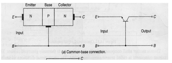
Common base configuration:
In this configuration base terminal is conncted as a common terminal. The input is applied between the emitter and base terminals.The output is taken between the collector and base terminals.
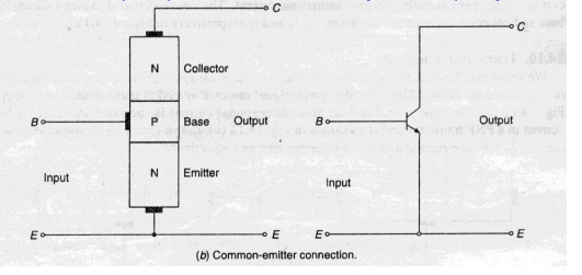
Common emitter configuration:
In this configuration emitter terminal is conncted as a common terminal.
The input is applied between the base and emitter terminals.The output is taken between the collector and base terminals.
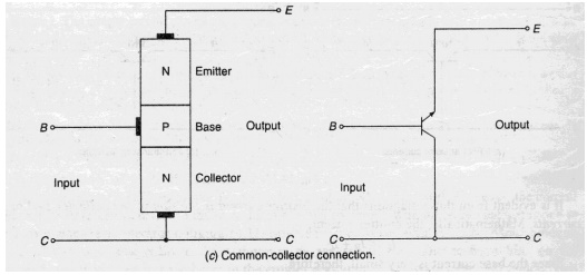
Common collector configuration:
In this configuration collector terminal is conncted as a common terminal.
The input is applied between the base and collector terminals.The output is taken between the emitter and collector terminals
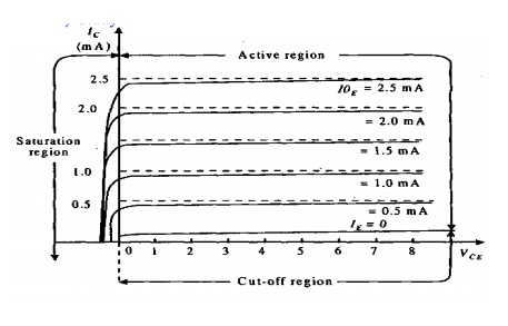
CB, CE,CC Characteristics :
1. Common base Characteristics :
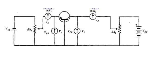
Input characteristics:
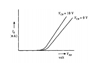
v The output(CB) voltage is maintained constant and the input voltage (EB) is set at several convenient levels. For each level of input voltage, the input current IE is recorded.
v IE is then plotted versus VEB to give the common-base input characteristics.
v The EB junction is essentially the same as a forward biased diode, therefore the current-voltage characteristics is essentially the same as that of a diode:
Output characteristics:
The emitter current IE is held constant at each of several fixed levels. For each fixed value of IE , the output voltage VCB is adjusted in convenient steps and the corresponding levels of collector current IC are recorded.
.For each fixed value of IE, IC is almost equal to IE and appears to remain constant when VCB is increased.
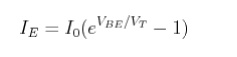
2.Common-Emitter Characteristics :
Input characteristics:
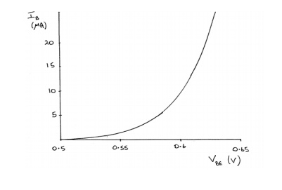
v The output voltage VCE is maintained constant and the input voltage VBE is set at several convenient levels.For each level of input voltage, the input current IB is recorded.
v IB is then plotted versus VBE to give the common-base input characteristics.
Output characteristics:
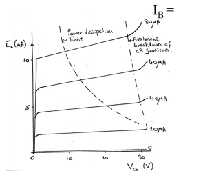
The Base current IB is held constant at each of several fixed levels. For each fixed value of IB , the output voltage VCE is adjusted in convenient steps and the corresponding levels of
collector current IC are recorded
v .For each fixed value of IB, IC level is Recorded at each VCE step.For each IB level, IC is plotted versus VCE to give a family of characteristics.
3.Common-Collector Characteristics :
![]()
Input characteristics:
v The common-collector input characteristics are quite different from either common base or common-emitter input characteristics.
v The difference is due to the fact that the input voltage (VBC)
is largely determined by (VEC) level .
VEC = VEB + VBC
VEB = VEC - VBC
Output characteristics:
The operation is much similar to that of C-E configuration.When the base current is ICO, the emitter current will be zero and consequently no current will flow in the load.
When the base current is increased, the transistor passes through active region and eventually reaches saturation.
Under the saturation conditions all the supply voltage, except for a very small drop across the transistor will appear across the load resistor.
Early Effect and Early Voltage
Base-Width Modulation:
v As reverse-bias across the collector-base junction increases, the width of the collector-base depletion layer increases and the effective width of base decreases.
v This is called ―base-width modulation‖.
Early effect:
When the output characteristics are extrapolated back to where the iC curves intersect at common point, vCE = -VA (Early voltage), which lies between 15 V and 150 V.
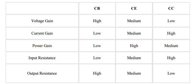
Comparison of the CB, CE, and CC Configurations
Related Topics