Chapter: VLSI Design : Specification Using Verilog HDL
Structural Gate Level Switch Level Modeling
STRUCTURAL GATE LEVEL SWITCH
LEVEL MODELING
Models of
MOS networks consist following four primitive types:
§ NMOS
§ PMOS
§ RNMOS
§ RPMOS
The pmos
keyword stands for PMOS transistor and the nmos keyword stands for NMOS
transistor. PMOS and NMOS transistors have relatively low impedance between
their sources and drains when they conduct.
The rpmos
keyword stands for resistive PMOS transistor and the rnmos keyword stands for
resistive NMOS transistor. Resistive PMOS and resistive NMOS transistors have
significantly higher impedance between their sources and drains when they
conduct than PMOS and NMOS transistors have. These four gate types are unidirectional
channels for data similar to the bufif gates.
Declarations
of these gates begin with one of the following keywords:
§ NMOS
§ PMOS
§ RNMOS
§ RPMOS
The delay
specification follows the keyword. A terminal list completes the declaration.
The delay specification can be 0, 1, 2, or 3 delays. If there is no delay,
there is no delay through the switch. A single delay determines the delay of
all output transitions.
If the
specification contains 2 delays, the first delay determines the rise delay, the
second delay determines the fall delay, and the smaller of t he 2 delays
specifies the delay of transitions to Z and X.
If there
are 3 delays, the first delay specifies the rise delay, the second delay
specifies the fall delay, the third delay determines the delay of transitions
to Z, and the smallest of the three delays applies to transitions to X. Delays
on transitions to H and L are the same as delays on transitions to X.
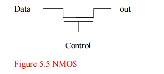
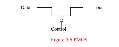
These
four switches have one output, one
data input, and one control input. The first terminal in the terminal
list connects to the output, the second terminal connects to the data input,
and the third terminal connects to the control input.
1. Switch level
modeling:
This is
another type of modeling used in verilog HDL. In this modeling, MOS switches
are used. In verilog HDL, transistors are also known as switches that either
conduct or are open.
Some
combinations of data input values and control input values cause these switches
to output either of two values, without a preference for either value. These
switches’ logic tables include 2 symbols representing such unknown results.
The
symbol L represents a result which has a value of 0 or Z. The symbol H
represents a result which has a value of 1 or Z.

2. Logic tables for
pmos, rpmos, nmos, and rnmos gates
The
following example declares a pmos switch:
pmos
(out, data, control);
The
output is out, the data input is data, and the control input is control.
3. Logic symbol: Nmos
switch
4. Pmos switch:
5. Bidirectional Pass
Switches
Declarations
of bidirectional switches begin with one of the following keywords:
tran
tranif1 tranif0 rtran rtranif1 rtranif0
Delay specification
follows the keywords
in declarations of
tranif1, tranif0, rtranif1, and
rtranif0;
the next item is the optional identifier. A terminal list completes the
declaration.
The delay
specifications for tranif1, tranif0, rtranif1, and rtranif0 devices can be 0,
1, or 2 delays. If there is no delay, the device has no turn-on or turn-off
delay. If the specification contains one delay, that delay determines both
turn-on and turn-off delays.
If there
are 2 delays, the first delay specifies the turn-on delay, and the second delay
specifies the turn- off delay These six devices do not delay signals
propagating through them. When these devices are turned off they block signals,
and when they are turned on they pass signals.
The
tranif1, tranif0, rtranif1, and rtranif0 devices have three items in their
terminal lists. Two are bidirectional terminals that conduct signals to and
from the devices, and the other terminal connects to a control input. The
terminals connected to inouts precede the terminal connected to the control
input in the terminal list.
The tran
and rtran devices have terminal lists containing two bidirectional terminals.
The
bidirectional terminals of all six of these devices connect only to scalar nets
or bit-selects of expanded vector nets.The following example declares a
tranif1:
tranif1
(inout1, inout2, control);The bidirectional terminals are inout1 and inout2.
The control input is control.
Related Topics