Chapter: Biotechnology Applying the Genetic Revolution: Nanobiotechnology
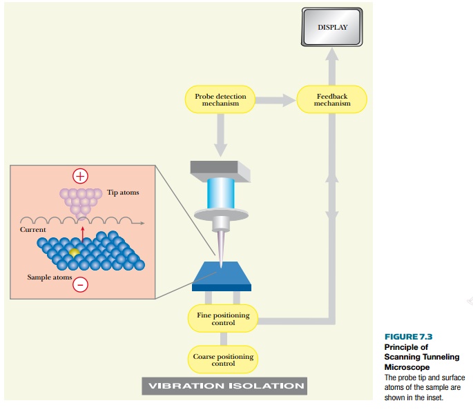
Scanning Tunneling Microscopy
SCANNING
TUNNELING MICROSCOPY
When a metal tip comes close
to a conducting surface, electrons can tunnel from one to the other, in either
direction. The probability of tunneling depends exponentially on the distance
apart. Surface contours can be mapped by keeping the current constant and
measuring the height of the tip above the surface. This allows resolution of
individual atoms on the surface being studied. This is the principle of the
scanning tunneling microscope (Fig. 7.3).
Atoms may also be moved using
the STM. In 1989, in perhaps the most famous experiment in nanotechnology, D.
M. Eigler and E. K. Schweizer fabricated the IBM logo by arranging 35 xenon
atoms on a nickel surface. They chose nickel because the valleys between rows
of nickel atoms are deep enough to hold xenon atoms in place, yet small enough
to allow the xenon atoms to be pulled over the surface. To move xenon atoms,
the STM tip was placed above a xenon atom, using imaging mode. Next, scanning
mode was turned off and the tip lowered until the tunneling current increased
severalfold (“fabrication mode”). The xenon atom was attracted to the STM tip
and was dragged by moving the tip horizontally. The atom was deposited at its
new location by reducing the tunneling current. Since then several diagrams
have been made in the same way. Carbon monoxide man is shown in Fig. 7.4.

From a biological perspective, the weakness of STM is that it requires a conducting surface, in practice generally a metal layer of some sort. The atomic force microscope (see following section) has the advantage of not needing conductive material and has therefore been more widely applied in biology.
Related Topics