Chapter: VLSI Design : CMOS Technology
CMOS Technologies
CMOS TECHNOLOGIES
CMOS
provides an inherently low power static circuit technology that has the
capability of providing a lower-delay product than comparable design-rule nMOS
or pMOS technologies. The four dominant CMOS technologies are:
§ P-well
process
§ n-well
process
§ twin-tub
process
§ Silicon
on chip process
1. The p-well process
A common
approach to p-well CMOS fabrication is to start with moderately doped n-type
substrate (wafer), create the p-type well for the n-channel devices, and build
the p-channel transistor in the native n-substrate. The processing steps are,
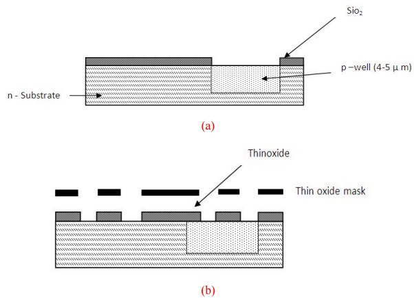
1.
The first mask defines the p-well (p-tub) n-channel
transistors (Fig. 1.4a) will be fabricated in this well. Field oxide (FOX) is
etched away to allow a deep diffusion.
2.
The next mask is called the “thin oxide” or
“thinox” mask (Fig. 1.4b), as it defines where areas of thin oxide are needed
to implement transistor gates and allow implantation to form p- or n-type
diffusions for transistor source/drain regions.
The field
oxide areas are etched to the silicon surface and then the thin oxide areas is
grown on these areas. O ther terms for this mask include active area, island,
and mesa.
3.
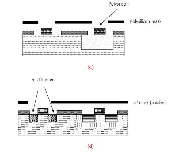
Polysilicon gate definition is then completed. This
involves covering the surface with polysilicon (Fig 1.4c) and then etching the
required pattern (in this case an inverted “U”). “Poly” gate regions lead to
“self-aligned” source-drain regions.
4.
A p-plus (p+) mask is then used to
indicate those thin-oxide areas (and polysilicon) that are to be implanted p+.
Hence a thin-oxide area exposed by the p-plus mask (Fig. 1.4d) will become a p+
diffusion area. If the p-plus area is in the n-substrate, then a
p-channel transistor or p- type wire may be constructed. If the p-plus area is
in the p-well, then an ohmic contact to the p-well may be constructed.
5. The
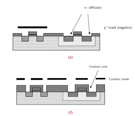
next step usually uses the complement of the p-plus mask, although an extra
mask is normally not needed. The “absence” of a p-plus region over a thin-oxide
area indicates that the area will be an n+ diffusion or n-thinox. n-thinox
in the p-well defines possible n transistors and wires. An n+
diffusion (Fig. 1.4e) in the n-substrate allows an ohmic contact to be made.
Following this step, the surface of the chip is covered with a layer of Sio2.
6.
Contacts cuts are then defined. This involves
etching any Sio2 down to the contacted surface, these allow metal (Fig. 1.4f)
to contact diffusion regions or polysilicon regions.
7.
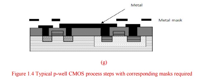
Metallization (Fig. 1.4g) is then applied to the
surface and selectively etched.
8.
As a final step, the wafer is passivated and
openings to the bond pads are etched to allow for wire bonding. Passivation
protects the silicon surface against the ingress of contaminants.
Basically
the structure consists of an n-type substrate in which p-devices may be formed
by suitable masking and diffusion and, in order to accommodate n-type devices,
a deep p-well is diffused into the n-type substrate.
This
diffusion must be carried out with special care since the p-well doping
concentration and depth will affect the threshold voltages as well as the
breakdown voltages of the n-transistors.
To
achieve low threshold voltage (0.6 to 1.0 V), deep well diffusion or high well
resistivity is needed.
However,
deep wells require larger spacing between the n- and p-type transistors and
wires because of lateral diffusion resulting in larger chip areas.
High
resistivity can accentuate latch-up problems. In order to achieve narrow
threshold voltage tolerances in a typical p-well process, the well
concentration is made about one order of magnitude higher than the substrate
doping density, thereby causing the body effect for n-channel devices to be
higher than for p-channel transistors.
In
addition, due to this higher concentration, n-transistors suffer from excessive
source/drain to p-well capacitance will tends to be slower in performance.
The well
must be grounded in such a way as to minimize any voltage drop due to injected
current in substrate that is collected by the p-well.
The
p-well act as substrate for then-devices within the parent n-substrate, and,
provided polarity restrictions are observed, the two areas are electrically
isolated such that there are in affect two substrate, two substrate connections
(VDD and VSS) are required.
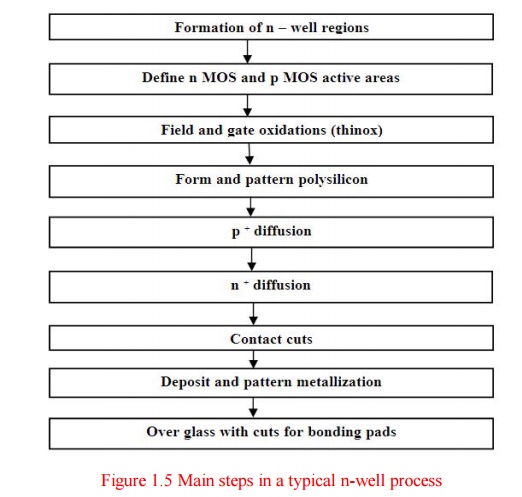
2. The n-well process
The
p-well processes have been one of the most commonly available forms of CMOS.
However, an advantage of the n-well process is that it can be fabricated on the
same process line as conventional n MOS.
n –well
CMOS circuits are also superior to p-well because of the lower substrate bias
effects on transistor threshold voltage and inherently lower parasitic
capacitances associated with source and drain regions.
Typically
n-well fabrication steps are similar to a p-well process, except that an n-well
is used which is illustrated in Fig. . The first masking step defines the
n-well regions.
This followed
by a low phosphorus implant driven in by a high temperature diffusion step to
form the n-wells.
The well
depth is optimized to ensure against p-substrate to p+ diffusion
breakdown without compromising the n-well to n+ mask separation.
The next
steps are to define the devices and diffusion paths, grow field oxide, deposit
and pattern the polysilicon, carry out the diffusions, make contact cuts and
metallization.
An n-well
mask is used to define n-well regions, as opposed to a p-well mask in a p-well
process.
An n-plus
(n+) mask may be used to define the n-channel transistors and VDD
contacts. Alternatively, we could use a p-plus mask to define the p-channel
transistors, as the masks usually are the complement of each other.
Due to
differences in mobility of charge carriers the n-well process creates
non-optimum p- channel characteristics, such as high junction capacitance and
high body effect. The n-well technology has a distinct advantage of providing
optimum device characteristics.
Thus
n-channel devices may be used to form logic elements to provide speed and
density, while p-transistors could primarily serve as pull-up devices.
3. The twin-tub process
Twin-tub
CMOS technology provides the basis for separate optimization of the p-type and
n-type transistors, thus making it possible for threshold voltage, body effect,
and the gain associated with n- and p-devices to be independently optimized.
Generally
the starting material is either an n+ or p+ substrate
with a lightly doped epitaxial or epi layer, which is used for protection
against latch-up.
The aim
of epitaxial is to grow high purity silicon layers of controlled thickness with
accurately determined dopant concentrations distributed homogeneously
throughout the layer. The electrical properties for this layer are determined
by the dopant and its concentration in the silicon.
The
process sequence, which is similar to the p-well process apart from the tub
formation where both p-well and n-well are utilized as in Fig. 1.7, entails the
following steps:
§ Tub
formation
§ Thin
oxide etching
§ Source
and drain implantations
§ Contact
cut definition
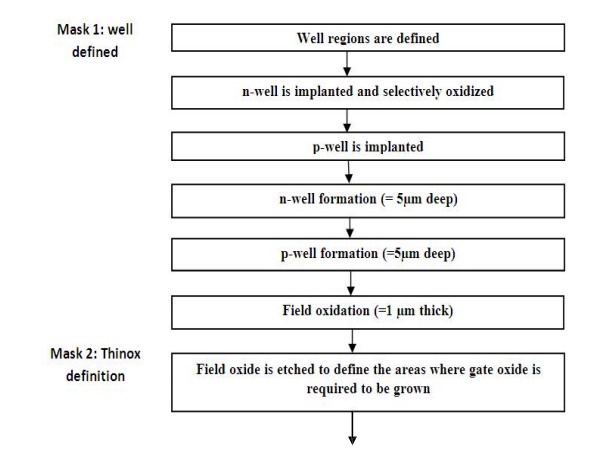
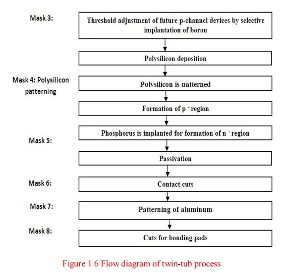
Since
this process provides separately optimized wells, better p erformance
n-transistors (lower capacitance, less body effect) may be constructed when
compared with a conventional p-well process.
Similarly
the p-transistors may be optimized. The use of threshold adjust steps is
included in this process.
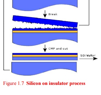
4. Silicon on insulator
process
Silicon on insulator (SOI) CMOS processes has several potential advantages such as higher density, no latch-up problems, and lower parasitic capacitances.
In the SOI process a thin layer of single crystal silicon film is epitaxial grown on an insulator such as sapphire or magnesium aluminates spinal. The steps involves are:
1) A thin
film (7-8 µ m) of very lightly doped n-type Si is grown over an insulator
Sapphire is a commonly used insulator.
2) An
anisotropic etch is used to etch away the Si except where a diffusion area will
be needed.
3) The
p-islands are formed next by masking the n-islands with a photo resist. A
p-type dopant (boron) is then implanted. It is masked by the photo resist and
at the u unmasked islands. The p-islands will become the n-channel devices.
4) The
p-islands are then covered with a photo resist and an n-type dopant,
phosphorus, is implanted to form the n-islands .The n-islands will become the
p-channel devices.
5) A thin
gate oxide (500-600Å ) is grown over all of the Si structures. This is normally
done by thermal oxidation.
6) A
polysilicon film is deposited over the oxide.
7) The
polysilicon is then patterned by photo masking and is etched. This defines the
polysilicon layer in the structure
8) The next
step is to form the n-doped source and drain of the n-channel devices in the p-
islands. The n-island is covered with a photo resist and an n-type dopant
(phosphorus) is implanted.
9) The
p-channel devices are formed next by masking the p-islands and implanting a
p-type dopant. The polysilicon over the gate of the n-islands will block the
dopant from the gate, thus forming the p-channel devices.
10) A layer
of phosphorus glass is deposited over the entire structure. The glass is etched
at contact cut locations. The metallization layer is formed. A final
passivation layer of a phosphorus glass is deposited and etched over bonding
pad locations.
5. The advantages
§ Due to
the absence of wells, denser structures than bulk silicon can be obtained.
§ Low
capacitances provide the basis of very fast circuits.
§ No
field-inversion problems exist.
§ No
latch-up due to isolation of n- and p- transistors by insulating substrate.
§ As there
is no conducting substrate, there are no body effect problems
§ Enhanced
radiation tolerance.
But the
drawback is due to absence of substrate diodes, the inputs are difficult to
protect. As device gains are lower, I/O structures have to be larger. Single
crystal sapphires are more expensive than silicon and processing techniques
tend to be less developed than bulk silicon techniques.
Related Topics