Operational Amplifiers - Voltage Sources | Linear Integrated Circuits : Basics of Operational Amplifiers
Chapter: Linear Integrated Circuits : Basics of Operational Amplifiers
Voltage Sources
Voltage
Sources
A
voltage source is a circuit that produces an output voltage V0,
which is independent of the load driven by the voltage source, or the output
current supplied to the load. The voltage source is the circuit dual of the
constant current source.
A
number of IC applications require a voltage reference point with very low ac
impedance and a stable dc voltage that is not affected by power supply and
temperature variations. There are two methods which can be used to produce a
voltage source, namely,
1.
Using
the impedance transforming properties of the transistor, which in turn
determines the current gain of the transistor and
2.
Using
an amplifier with negative feedback.
Voltage source circuit using Impedance transformation:
The
voltage source circuit using the impedance transforming property of the
transistor is shown in figure. The source voltage Vs drives the base of the
transistor through a series resistance RS and the output is taken
across the emitter. From the circuit, the output ac resistance looking Into
emitter is given by
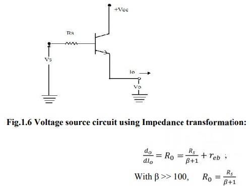
It
is to be noted that, equation is applicable only for small changes in the
output current. The load regulation parameter indicates the changes in V0
resulting from large changes in output current I0 , Reduction in V0
occurs as I0 goes from no-load current to full-load current and this
factor determines the output impedance of the voltage sources.
Emitter– follower or Common Collector Type Voltage source:
The
figure shows an emitter follower or common collector type voltage source.
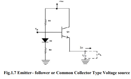
This
voltage source is suitable for the differential gain stage used in op-amps.
This circuit has the advantages of
A. Producing low ac impedance and
B. Resulting in effective decoupling of
adjacent gain stages.
The
low output impedance of the common-collector stage simulates a low impedance
voltage
source
with an output voltage level of V0 represented= by
The
diode D1 is used for offsetting the effect of dc value VBE , across
the E-B junction of the transistor, and for compensating the temperature
dependence of VBE drop of Q1. The load ZL
shown in dotted line represents the circuit biased by the current through Q1.
The
impedance R0 looking into the emitter= of Q1 derived from the hybrid π model
is given by
Voltage Source Using Temperature compensated Avalanche Diode
The
voltage source using common collector stage has the limitations of its
vulnerability for changes in bias voltage VN and the output voltage
V0 with respect to changes in supply voltage Vcc. This is overcome in the
voltage source circuit using the breakdown voltage of the base- emitter
junction shown below.
The
emitter – follower stage of common – collector is eliminated in this circuit,
since the impedance seen looking into the bias terminal N is very low. The
current source I1 is normally simulated by a resistor connected
between Vcc and node n. Then, the output voltage level V0 at node N is given by
V0 = VB +VBE Where VB is the breakdown
voltage of diode DB and VBE is the diode drop across D1.
The
breakdown diode DB is normally realized using the base-emitter
junction of the transistor. The diode D1 provides partial
compensation for the positive temperature coefficient effect of VB.
In a monolithic IC structure, DB and D1 can be
conveniently realized as a single transistor with two individual emitters as
shown in figure.
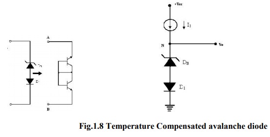
Voltage source using breakdown voltage of the base- emitter junction
The
structure consists of composite connection of two transistors which are
diode-connected back-to back. Since the transistors have their base to
collector terminals common, they can be designed as a single transistor with
two emitters.
The
output resistance R0 looking into the output terminal in figure is given by Ro=RB+VT/I1
where RB and VT/I1 are the ac resistances of
the base–emitter resistance of diode DB and D1
respectively. Typically RB is in the range of 40Ω to 100Ω, and V0 in the range
of 6.5V to 9V.
Voltage Source using VBE as a reference:
The output stage of op-amp requires
stabilized bias voltage source, which can be obtained using a forward-biased
diode connected transistor. The forward voltage drop for such a connection is
approximately 0.7V, and it changes slightly with current.
When a voltage level greater than 0.7V,
is needed, several diodes can be connected in series, which can offer integral
multiples of 0.7V. Alternatively, the figure shows a multiplier circuit, which
can offer voltage levels that need not be integral multiplied of 0.7V. The drop
across R2 equals VBE drop of Q1. Considering negligible base current
for Q1, current through R2 is the same as that flowing through R1.
Therefore, the output voltage V0
can be expressed as
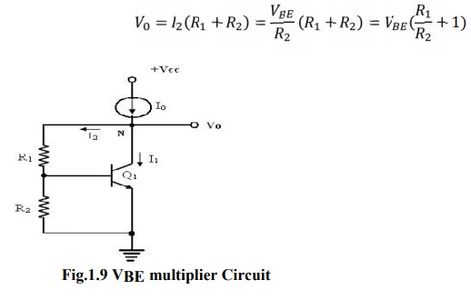
Hence,
the voltage V0 can be any multiple of VBE by properly
selecting the resistors R1 and R2. Due to the shunt
feedback provided by R1, the transistor current I1 automatically
adjusts itself, towards maintaining I2 and V0 relatively
independent of the changes in supply voltage.
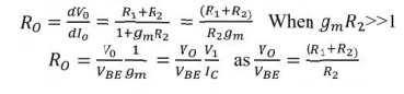
The ac output resistance of the circuit R0
is given= by,
Related Topics