Operational Amplifiers - Voltage References | Linear Integrated Circuits : Basics of Operational Amplifiers
Chapter: Linear Integrated Circuits : Basics of Operational Amplifiers
Voltage References
Voltage
References
The
circuit that is primarily designed for providing a constant voltage independent
of changes in temperature is called a voltage reference. The most important
characteristic of a voltage reference is the temperature coefficient of the
output= reference voltage TcR ,
and it is expressed as

The
desirable properties of a voltage reference are:
1.
Reference
voltage must be independent of any temperature change.
2.
Reference
voltage must have good power supply rejection which is as independent of the
supply voltage as possible and
3.
Output
voltage must be as independent of the loading of output current as possible, or
in other words, the circuit should have low output impedance.
The
voltage reference circuit is used to bias the voltage source circuit, and the
combination can be called as the voltage regulator. The basic design strategy
is producing a zero TCR at a given temperature, and thereby achieving good
thermal ability. Temperature stability of the order of 100ppm/0 C is
typically expected.
Voltage Reference circuit using temperature compensation scheme
The
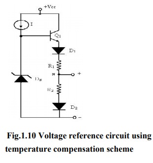
voltage reference circuit using basic temperature compensation scheme is shown
below. This design utilizes the close thermal coupling achievable among the
monolithic components and this technique compensates the known thermal drifts
by introducing an opposing and compensating drift source of equal magnitude.

A
constant current I is supplied to the avalanche diode DB and it
provides a bias voltage of VB to the base of Q1. The
temperature dependence of the VBE drop across Q1 and
those across D1 and D2 results in respective temperature
coefficients. Hence, with the use of resistors R1 and R2
with tapping across them at point N compensates for the temperature drifts in
the base-emitter loop of Q1. This results in generating a voltage
reference VR with normally zero temperature coefficient.
Voltage Reference circuit using Avalanche Diode Reference:
A
voltage reference can be implemented using the breakdown phenomenon condition
of a heavily doped PN junction. The Zener breakdown is the main mechanism for
junctions, which breakdown at a voltage of 5V or less. For integrated
transistors, the base-emitter breakdown voltage falls in the range of 6 to 8V.
Therefore, the breakdown in the junctions of the integrated transistor is
primarily due to avalanche multiplication. The avalanche breakdown voltage VB
of a transistor incurs a positive temperature coefficient, typically in the
range of 2mV/0 C to 5mV/0 C.
Figure
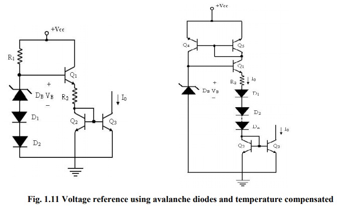
depicts a current reference circuit using avalanche diode reference. The base
bias for transistor Q1 is provided through register R1
and it also provides the dc current needed to bias DB, D1 and D2
. The voltage at the base of Q1 is equal to the Zener voltage VB
added with two diode drops due to D1 and D2. The voltage
across R2 is equal to the voltage at the base of Q1 less
the sum of the base – emitter voltages of Q1 and Q2.

Hence,
the voltage across R2 is approximately equal to that across DB
= VB. Since Q2 and Q3 act as a current mirror
circuit, current I0 equals the current through R2.
I0 = VB/R2
It
shows that, the output current I0 has low temperature coefficient,
if the temperature coefficient of R2 is low, such as that produced
by a diffused resistor in IC fabrication.
The
zero temperature coefficients for output current can be achieved, if diodes are
added in series with R2, so that they can compensate for the
temperature variation of R2 and VB. The temperature
compensated avalanche diode reference source circuit is shown in figure. The
transistor Q4 and Q5 form an active load current mirror
circuit. The base voltage of Q1 is the voltage VB across
Zener DB.
Then,
VB = (VBE * n) +VBE across Q1 + VBE
across Q2 + drop across R2. Here, n is the number of
diodes.
It
can be expressed as VB = ( n+ 2) VBE - I0 * R2
Differentiating
for VB, I0, R2 and VBE +partially,2
with respect to temperature T, we get

Dividing
throughout by I0 R2
, we get

Therefore,
zero temperature coefficient of I0 can be obtained, if the above
condition is satisfied.
Related Topics