Chapter: Linear Integrated Circuits : Basics of Operational Amplifiers
AC Characteristics of Operational Amplifiers
AC
Characteristics:
For
small signal sinusoidal (AC) application one has to know the ac characteristics
such as frequency response and slew-rate.
1. Frequency Response:
The
variation in operating frequency will cause variations in gain magnitude and
its phase angle. The manner in which the gain of the op-amp responds to
different frequencies is called the frequency response. Op-amp should have an
infinite bandwidth BW =∞ (i.e.) if its open loop gain in 90dB with dc signal
its gain should remain the same 90 dB through audio and onto high radio
frequency. The op-amp gain decreases (roll-off) at higher frequency what
reasons to decrease gain after a certain frequency reached. There must be a
capacitive component in the equivalent circuit of the op-amp. For an op-amp
with only one break (corner) frequency all the capacitors effects can be
represented by a single capacitor C. Below fig is a modified variation of the
low frequency model with capacitor C at the output.
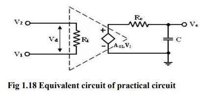
There
is one pole due to R0C and one -20dB/decade. The open loop voltage
gain of an op-amp with only one corner frequency is obtained from above fig.
f1
is the corner frequency or the upper 3 dB frequency of the op-amp. The
magnitude and phase angle of the open loop volt gain are f1 of frequency can be
written as, The magnitude and phase angle characteristics:
1.
For
frequency f<< f1 the magnitude of the gain is 20 log AOL in
db.
2.
At
frequency f = f1 the gain in 3 dB down from the dc value of AOL in
db. This frequency f1 is called corner frequency.
3.
For
f>> f1 the fain roll-off at the rate off -20dB/decade or
-6dB/decade.
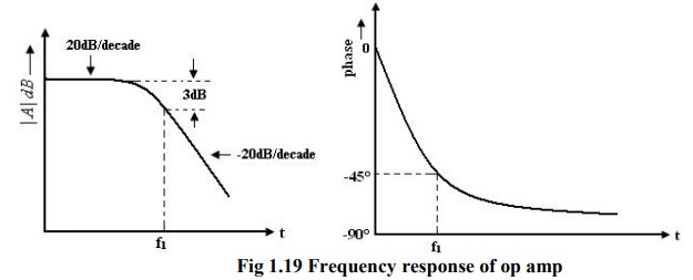
From
the phase characteristics that the phase angle is zero at frequency f = 0. At
the corner frequency f1 the phase angle is -45º![]()
![]() (lagging and an infinite frequency the phase
angle is -90
(lagging and an infinite frequency the phase
angle is -90![]() . It shows that a maximum of 90
. It shows that a maximum of 90![]()
![]() phase change can occur in an op-amp with a
single capacitor C. Zero frequency is taken as the decade below the corner
frequency and infinite frequency is one decade above the corner frequency.
phase change can occur in an op-amp with a
single capacitor C. Zero frequency is taken as the decade below the corner
frequency and infinite frequency is one decade above the corner frequency.
2. Circuit Stability:
A
circuit or a group of circuit connected together as a system is said to be
stable, if its o/p reaches a fixed value in a finite time. A system is said to
be unstable, if its o/p increases with time instead of achieving a fixed value.
In fact the o/p of an unstable sys keeps on increasing until the system break
down. The unstable system is impractical and need be made stable. The criterion
gn for stability is used when the system is to be tested practically. In
theoretically, always used to test system for stability, ex: Bode plots.
Bode
plots are compared of magnitude Vs Frequency and phase angle Vs frequency. Any
system whose stability is to be determined can represented by the block
diagram.
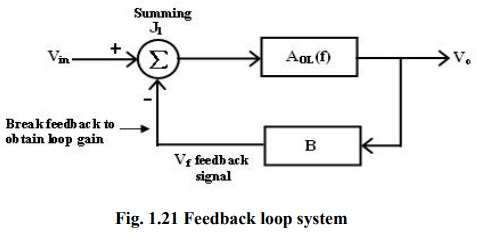
The
block between the output and input is referred to as forward block and the
block between the output signal and f/b signal is referred to as feedback
block. The content of each block is referred as transfer frequency. From fig.
we represented it by AOL (f) which is given by
AOL
(f) = V0/Vin if Vf = 0 ----- (1)
where
AOL (f) = open loop volt gain.
The
closed loop gain Af is given by AF = V0/Vin
=
AOL / (1+(AOL ) (B)
----(2)
B
= gain of feedback circuit.
B
is a constant if the feedback circuit uses only resistive components.
Once
the magnitude Vs frequency and phase angle Vs frequency plots are drawn, system
stability may be determined as follows
1. Method 1:
Determine
the phase angle when the magnitude of (AOL) (B) is 0dB (or) 1.
If
phase angle is >-180![]() , the system is stable. However, the some
systems the magnitude may never be 0, in that cases method 2, must be used.
, the system is stable. However, the some
systems the magnitude may never be 0, in that cases method 2, must be used.
2. Method 2:
Determine
the phase angle when the magnitude of (AOL) (B) is 0dB (or) 1.
If
phase angle is > - 180![]() , If the magnitude is –ve decibels then the
system is stable. However, the some systems the phase angle of a system may
reach -1800, under such conditions method 1 must be used to determine the
system stability.
, If the magnitude is –ve decibels then the
system is stable. However, the some systems the phase angle of a system may
reach -1800, under such conditions method 1 must be used to determine the
system stability.
3. DC Characteristics of op-amp:
Current
is taken from the source into the op-amp inputs respond differently to current
and
voltage
due to mismatch in transistor.
DC
output voltages are,
·
Input
bias current
·
Input
offset current
·
Input
offset voltage
·
Thermal
drift
Input bias current:
The
op-amp‘s input is differential amplifier, which may be made of BJT or FET.
In
an ideal op-amp, we assumed that no current is drawn from the input terminals
the base currents entering into the inverting and non-inverting terminals (IB-
& IB+ respectively).
Even
though both the transistors are identical, IB- and IB+
are not exactly equal due to internal imbalance between the two inputs.
Manufacturers specify the input bias current IB
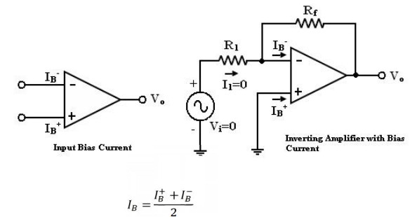
If input voltage Vi = 0V. The
output Voltage Vo should also be (Vo = 0) but for IB =
500nA We find that the output voltage is offset by Op-amp with a 1M feedback resistor
Vo = 500nA X 1M = 500mV
The output is driven to 500mV with zero
input, because of the bias currents.
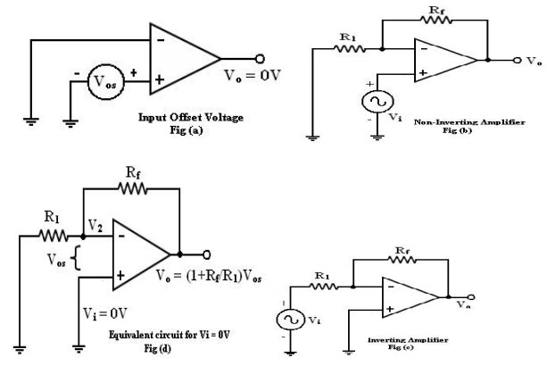
In application where the signal levels
are measured in mV, this is totally unacceptable. This can be compensated by a
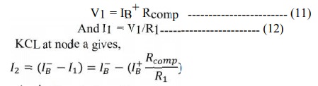
compensation resistor Rcomp has been added between the non-inverting
input terminal and ground as shown in the figure below.
Current
IB+ flowing through the compensating resistor Rcomp,
then by KVL we get,
- V1+0+V2-Vo
= 0 (or)
Vo = V2 – V1 ---------
(1)
By selecting proper value of Rcomp,
V2 can be cancelled with V1 and the Vo = 0.
The value of Rcomp is derived as
V1 = IB+Rcomp (or)
IB+ = V1/Rcomp
------------------------ (2)
The node ‘a’ is at voltage (-V1).
Because the voltage at the non-inverting input terminal is (-V1). So
with Vi = 0 we get,
I1 = V1/R1
------------------------ (3)
I2 = V2/Rf
------------------------ (4)
For
compensation, Vo should equal to zero (Vo = 0, Vi
= 0). i.e. from equation (3) V2 = V1. So that,
I2
= V1/Rf ——> (5)
KCL
at node ‘a’ gives,
IB-
= I2 + I1 =( V1/Rf ) +(V1/R1)
= V1(R1+Rf)/R1Rf ------------------------ (5)
Assume
IB- = IB+ and using equation (2)
& (5) we get
V1
(R1+Rf)/R1Rf = V1/Rcomp
Rcomp
= R1 || Rf ------------------------
(6)
i.e.
to compensate for bias current, the compensating resistor, Rcomp should be
equal to the parallel combination of resistor R1 and Rf.
Input offset current:
ü
Bias
current compensation will work if both bias currents IB+
and IB- are equal.
ü
Since
the input transistor cannot be made identical. There will always be some small
difference
between IB+ and IB-. This
difference is called the offset current
|Ios|
= IB+-IB-------------------------
(7)
Offset
current Ios for BJT op-amp is 200nA and for FET op-amp is 10pA. Even
with bias current compensation, offset current will produce an output voltage
when Vi = 0.
Again
V0 = I2 Rf – V1
Vo
= I2 Rf - IB+ Rcomp
Vo
= 1M Ω X 200nA
Vo
= 200mV with Vi = 0
Equation (16) the offset current can be
minimized by keeping feedback resistance small.
·
Unfortunately to obtain high input
impedance, R1 must be kept large.
·
R1 large, the feedback resistor Rf must
also be high. So as to obtain reasonable gain.
The T-feedback network is a good
solution. This will allow large feedback resistance, while keeping the
resistance to ground low (in dotted line).
·
The T-network provides a feedback signal
as if the network were a single feedback resistor.
By T to Π conversion,
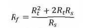
To design T- network first pick
Rt<<Rf/2 and=calculate
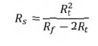
Input offset voltage:
In
spite of the use of the above compensating techniques, it is found that the
output voltage may still not be zero with zero input
voltage [Vo ≠ 0 with Vi= 0]. This is due to unavoidable imbalances inside the
op-amp and one may have to apply a small voltage at the input terminal to make
output (Vo) = 0.
This voltage is called input offset
voltage Vos. This is the voltage required to be applied at the input for making
output voltage to zero (Vo = 0).
Let
us determine the Vos on the output of inverting and non-inverting amplifier. If
Vi = 0 (Fig (b) and (c)) become the same as in figure (d).
Total output offset voltage:
The
total output offset voltage VOT could be either more or less than
the offset voltage produced at the output due to input bias current (IB)
or input offset voltage alone(Vos). This is because IB and Vos could
be either positive or negative with respect to ground. Therefore the maximum
offset voltage at the output of an inverting and non-inverting amplifier
(figure b, c) without any compensation technique used is given by many op amps
provide offset compensation pins to nullify the offset voltage. A 10K
potentiometer is placed across offset null pins 1&5. The wipes connected to
the negative supply at pin 4. The position of the wipes is adjusted to nullify
the offset voltage.
When the given (below) op-amps does not
have these offset null pins, external balancing techniques are used.
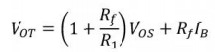
With
Rcomp, the total output offset
Balancing
circuit: Inverting amplifier:
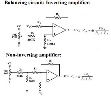
Non-inverting
amplifier:
Thermal drift:
Bias
current, offset current, and offset voltage change with temperature. A circuit
carefully nulled at 25ºC may not remain. So when the temperature rises to 35ºC.
This is called drift. Offset current drift is expressed in nA/ºC. These
indicate the change in offset for each degree Celsius change in temperature.
Related Topics