Operational Amplifiers - Closed loop op-amp configuration | Linear Integrated Circuits : Basics of Operational Amplifiers
Chapter: Linear Integrated Circuits : Basics of Operational Amplifiers
Closed loop op-amp configuration
Closed
– loop op-amp configuration:
The
op-amp can be effectively utilized in linear applications by providing a
feedback from the output to the input, either directly or through another
network. If the signal feedback is out- of-phase by 1800 with respect to the
input, then the feedback is referred to as negative feedback or degenerative
feedback. Conversely, if the feedback signal is in phase with that at the
input, then the feedback is referred to as positive feedback or regenerative
feedback.
An
op – amp that uses feedback is called a closed – loop amplifier. The most commonly
used closed – loop amplifier configurations are 1. Inverting amplifier (Voltage
shunt amplifier) 2. Non- Inverting amplifier (Voltage – series Amplifier)
Inverting Amplifier:
The
inverting amplifier is shown in figure and its alternate circuit arrangement is
shown in figure, with the circuit redrawn in a different way to illustrate how
the voltage shunt feedback is achieved. The input signal drives the inverting
input of the op – amp through resistor R1.
The
op – amp has an open – loop gain of A, so that the output signal is much larger
than the error voltage. Because of the phase inversion, the output signal is
1800 out – of – phase with the input signal. This means that the feedback
signal opposes the input signal and the feedback is negative or degenerative.
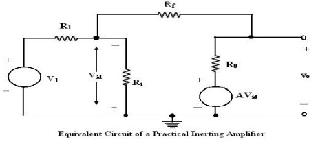
Practical Inverting amplifier:
The
practical inverting amplifier has finite value of input resistance and input
current, its open voltage gain A0 is less than infinity and its
output resistance R0 is not zero, as against the ideal inverting amplifier
with finite input resistance, infinite open – loop voltage gain and zero output
resistance respectively.
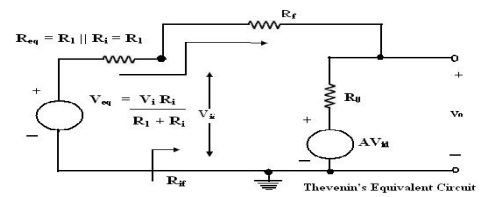
Figure
shows the low frequency equivalent circuit model of a practical inverting
amplifier. This circuit can be simplified using the Thevenin‘s equivalent
circuit shown in figure. The signal source Vi and the resistors R1
and Ri are replaced by their Thevenin‘s equivalent values. The closed – loop
gain AV and the input impedance Rif are calculated as follows.
The
input impedance of the op- amp is normally much larger than the input
resistance R1.
Therefore,
we can assume Veq ≈ Vi and Req ≈ R1 . From the figure
V0
= IR0 = AVid
Vid=
IRf = AVid
V0
= IR0 = AVid
Substituting
the0 valuef of I derived from above eqn. and obtaining the closed loop gain. It
can be observed from above eqn. that when A>> 1, R0 is negligibly small
and the product AR1 >> R0 +Rf , the
closed loop gain is given by
Av
= − Rf/R1
Which
as the same form as given in above eqn for an ideal inverter.
Input Resistance:
Rif
= Vid/ I1 =(Rf+R0)/(1+A)
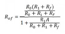
Output Resistance:
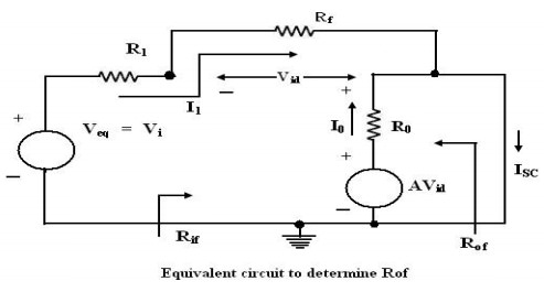
Figure
shows the equivalent circuit to determine Rof. The output impedance
Rof without the load resistance factor RL is calculated from the
open circuit output voltage Voc and the short circuit output current
ISC.
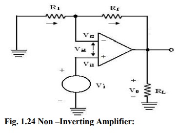
Non –Inverting Amplifier:
The
non – inverting Amplifier with negative feedback is shown in figure. The input
signal drives the non – inverting input of op-amp. The op-amp provides an
internal gain A. The external resistors R1 and Rf form the feedback voltage
divider circuit with an attenuation factor of β.
Since
the feedback voltage is at the inverting input, it opposes the input voltage at
the non – inverting input terminals, and hence the feedback is negative or
degenerative.
The
differential voltage Vid at the input of the op-amp is zero, because
node A is at the same voltage as that of the non- inverting input terminal. As
shown in figure, Rf and R1 form a potential divider.
Therefore,
Closed Loop Non – Inverting Amplifier
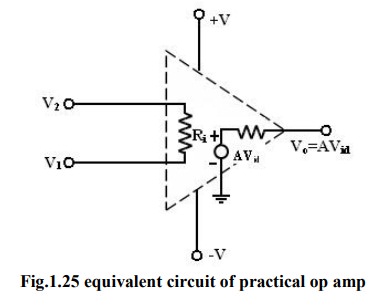
The
input resistance of the op – amp is extremely large (approximately infinity,)
since the op – amp draws negligible current from the input signal.
Practical Non –inverting amplifier:
The
equivalent circuit of a non- inverting amplifier using the low frequency model
is shown below in figure. Using Kirchhoff’s current law at node a,
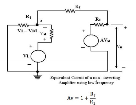
The
difference volt is equal to the input volt minus the f/b volt. (or) The
feedback volt always opposes the input volt (or out of phase by 1800 with respect
to the input voltage) hence the feedback is said to be negative.
It
will be performed by computing
1. Closed loop volt gain
2. Input and output resistance
3. Bandwidth
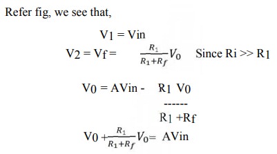
1. Closed loop volt gain:
The
closed loop volt gain is AF = V0 /Vin
V0
= Avid =A(V1 –V2 )
A
= large signal voltage gain.
From
the above eqn.
V0
= A(V1 – V2 )
Related Topics