Chapter: Digital Principles and System Design : Memory and Programmable Logic
Two Types of Memories
MEMORY AND PROGRAMMABLE LOGIC
PRE-REQUISITE DISCUSSION
A memory unit is a device
to which binary information is transferred for storage and from which
information is retrieved when needed for processing. When data processing takes
place, information from memory is transferred to selected registers in the
processing unit. A memory unit is a collection of cells capable of storing a
large quantity of binary information.
Communication between memory and
its environment is achieved through data input and output lines, address
selection lines, and control lines that specify the direction of transfer.
TWO TYPES OF MEMORIES
There are two types of memories that are used in digital systems: random-access memory (RAM) and read-only memory (ROM) The process of storing new information into memory is referred to as a memory “write” operation. The process of transferring the stored information out of memory is referred to as a memory “read” operation. RAM can perform both write and read operations. ROM can perform only the read operation. This means that suitable binary information is already stored inside memory and can be retrieved or read at any time. However, that information cannot be altered by writing.
ROM is one example of a PLD. Other such units are
the programmable logic array (PLA) - Programmable array logic (PAL), and the
field -programmable gate array (FPGA). A PLD is an integrated circuit with
internal logic gates connected through electronic paths that behave similarly
to fuses.

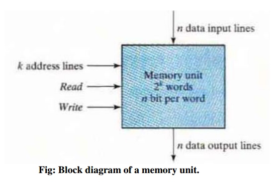
Fig:
Block diagram of a memory unit.
The n data input lines provide the information to
be stored in memory and the n data output lines supply the information coming
out of memory. The k address lines specify the particular word chosen among the
many available. The two control inputs specify the direction of transfer
desired: The Write input causes binary data to be transferred into the memory
and the Read input causes binary data to be transferred out of memory.
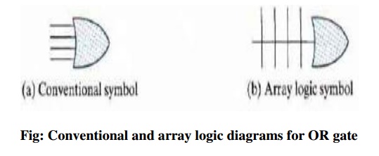
A typical PLD may have hundreds to millions of
gates interconnected through hundreds to thousands of internal paths. Instead
of having multiple input lines into the gate, we draw a single line entering
the gate. The input lines are drawn perpendicular to this single line and are
connected to the gate through internal fuses as shown in the figure. In a similar
fashion, we can draw the array logic for an AND gate.

Related Topics