Chapter: Digital Principles and System Design : Memory and Programmable Logic
Sequential programmable devices
SEQUENTIAL PROGRAMMABLE
DEVICES
Digital systems are designed with flip-flops and gates. Since
the combinational PLD consists of only gates, it is necessary to include
external flip-flops when they are used in the design. Sequential programmable
devices include both gates and flip-flops.

1. Sequential
(or simple) programmable logic device (SPLD)
2. Complex
programmable logic device (CPLD)
3. Field-programmable
gate array (FPGA)

The ever-increasing capacity of integrated circuits created an
opportunity for IC manufacturers to design larger PLDs for larger
digital-design applications. Instead, IC manufacturers devised complex PLD
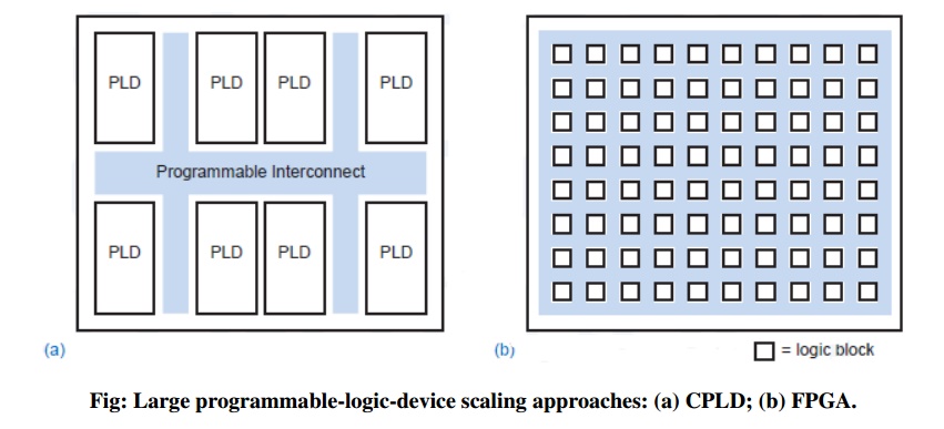
(CPLD) architectures to achieve the required scale. A typical CPLD is merely a
collection of multiple PLDs and an interconnection structure, all on the same
chip. In addition to the individual PLDs, the on-chip interconnection structure
is also programmable, providing a rich variety of design possibilities. CPLDs
can be scaled to larger sizes by increasing the number of individual PLDs and
the richness of the interconnection structure on the CPLD chip.
At about the same time that CPLDs were being invented, other
IC manufacturers took a different approach to scaling the size of programmable
logic chips. Compared to a CPLD, a field-programmable gate arrays (FPGA)
contains a much larger number of smaller individual logic blocks, and provides
a large, distributed interconnection structure that dominates the entire chip.

Field-Programmable
Gate Arrays
Even larger devices, often called field-programmable gate arrays (FPGAs), use read/write memory cells to control the state of each connection. The read/write memory cells are volatile— they do not retain their state when power is removed. Therefore, when power is first applied to the FPGA, all of its read/write memory must be initialized to a state specified by a separate, external nonvolatile memory. This memory is typically either a programmable read-only memory (PROM) chip attached directly to the FPGA or it’s part of a microprocessor subsystem that initializes the FPGA as part of overall system initialization.
Related Topics