Chapter: Digital Principles and System Design : Memory and Programmable Logic
Random Access Memory(RAM)
RANDOM ACCESS MEMORY
A memory unit is a collection of storage cells together with
associated circuits needed to transfer information into and out of a device.
The time it takes to transfer information to or from any desired random
location is always the same-hence the name random access memory, abbreviated as
RAM.
A memory unit stores binary information in groups of bits
called words. A word in memory is an entity of bits that move in and out of
storage as a unit. A memory word is a group of 1 's and 0's and may represent a
number, an instruction , one or more alphanumeric characters or any other
binary-coded information. A group of 8 bits is called a byte. Most computer
memories use words that are multiples of 8 bits in length.
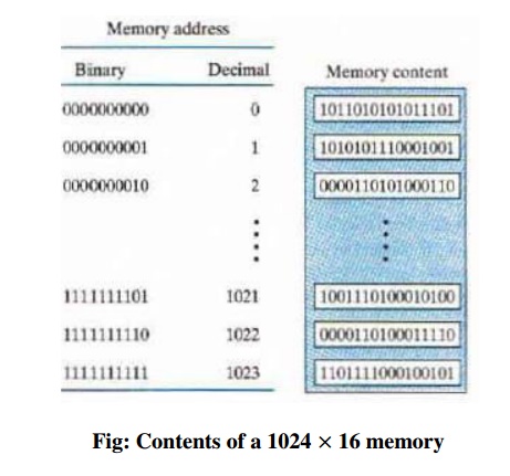
Each word in memory is assigned
an identification number called an address starting from 0 upto 2k-1.
where k is the number of address lines. Consider for example, a memory unit
with a capacity of 1K words of 16 bits each. Since 1K=1024 = 210 and
16 bits constitute two bytes, we can say that the memory can accommodate 2048 =
2K bytes.
Read and write operations- The two
operations that RAM can perform are the write and read operations. The
steps that must be taken for the purpose of transferring a new word to be
stored into memory are as follows:
·
Apply the binary address of the desired word to
the address lines.
· Apply the data bits that must be
stored in memory to the data input lines.
·
Activate the write input.
The memory unit will then take
the bits from the input data lines and store them in the word specified by the
address lines. The steps that must be taken for the purpose of transferring a
stored word out of memory are as follows:
· Apply the binary address of the
desired word to the address lines.
·
Activate the read input.
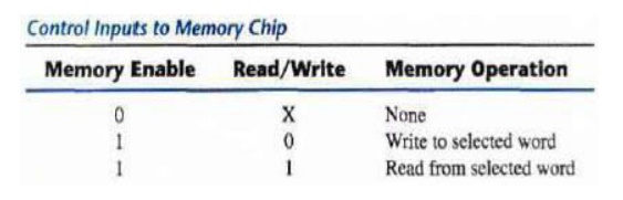
The memory enable (sometimes
called the chip select) is used to enable the particular memory chip in a
multichip implementation of a large memory. When the memory enable is inactive,
the memory chip is not selected and no operation is performed. When the memory
enable input is active, the read/write input determines the operation to be
performed.
Timing Waveforms
The operation of the memory unit
is controlled by an external device such as a central processing unit (CPU).
The CPU is usually synchronized by its own clock .The memory however doesn’temploy an
internal clock. Instead it’sread and
write operations are specified by control inputs.
The access time of memory is the time required to
select a word and read it. The cycle time of memory is the time required to
complete a write operation.
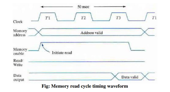
The read cycle shown in figure has an address for the memory
provided by the CPU. The memory-enable and read/write signals must be in their
high level for a read operation. The memory places the data of the word
selected by the address into the output data lines within a 50-ns interval (or
less) from the time that the memory enable is activated. The CPU can transfer
the data into one of its internal registers during the negative transition of
T3.The next T1 cycle is available for another memory request.
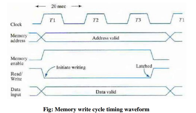
For a write operation, the CPU
must provide the address and input data to the memory. This is done at the
beginning of TI. The memory enable and the read/write signals must be activated
after the signals in the address lines are stable in order to avoid destroying
data in other memory words.
The memory enable signal switches
to the high level and the read/write signal switches to the low level to
indicate a write operation. The two control signals must stay active for at
least 50 ns. The address and data signals must remain stable for a short time
after the control signals are deactivated. At the completion of the third clock
cycle, the memory write operation is completed and the CPU can access the
memory again with the next TI cycle.
Types of RAM
Integrated circuit RAM units are
available in two operating modes: static and dynamic. Static RAM (SRAM)
consists essentially of internal latches that store the binary information.
The stored information remains valid as long as power is applied to the
unit. Dynamic RAM (DRAM) stores the binary information in the form of
electric charges on capacitors provided inside the chip by MOS transistors.
The stored charge on the capacitors tends to discharge with
time, and the capacitors must be periodically recharged by refreshing the
dynamic memory. Refreshing is done by cycling through the words every
few milliseconds to restore the decaying charge. DRAM offers reduced power
consumption and larger storage capacity in a single memory chip. SRAM is easier
to use and has shorter read and write cycles.
ROM is another nonvolatile memory. A nonvolatile memory
enables digital computers to store programs
that will be needed again after the computer is turned on.
Programs and data that cannot be altered are stored in ROM, while other large
programs are maintained on magnetic disk.
Related Topics