Functional block diagram, Output waveform, Pin description, Applications - The 555 Timer IC | Linear Integrated Circuits : Waveform Generators and Special Function ICs
Chapter: Linear Integrated Circuits : Waveform Generators and Special Function ICs
The 555 Timer IC
The 555
Timer IC
The
555 is a monolithic timing circuit that can produce accurate & highly
stable time delays or oscillation. The timer basically operates in one of two
modes: either
(i) Monostable (one - shot)
multivibrator or
(ii) Astable (free running) multivibrator
The
important features of the 555 timer are these:
(i) It operates on +5v to +18 v supply
voltages
(ii) It has an adjustable duty cycle
(iii) Timing is from microseconds to hours
(iv) It has a current o/p
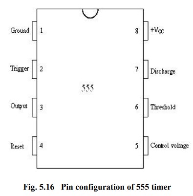
Pin description:
Pin
1: Ground:
All
voltages are measured with respect to this terminal.
Pin
2: Trigger:
The
o/p of the timer depends on the amplitude of the external trigger pulse applied
to this pin.
Pin
3: Output:
There
are 2 ways a load can be connected to the o/p terminal either between pin3
& ground or between pin 3 & supply voltage
(Between
Pin 3 & Ground ON load) (BetweenPin 3 & + Vcc OFF load)
(i) When the input is low:
The
load current flows through the load connected between Pin 3 & +Vcc in to
the output terminal & is called the sink current.
(ii) When the output is high:
The
current through the load connected between Pin 3 & +Vcc (i.e. ON load) is
zero. However the output terminal supplies current to the normally OFF load.
This current is called the source current.
Pin
4: Reset:
The
555 timer can be reset (disabled) by applying a negative pulse to this pin.
When the reset function is not in use, the reset terminal should be connected
to +Vcc to avoid any false triggering.
Pin
5: Control voltage:
An
external voltage applied to this terminal changes the threshold as well as
trigger voltage. In other words by connecting a potentiometer between this pin
& GND, the pulse width of the output waveform can be varied. When not used,
the control pin should be bypassed to ground with 0.01 capacitor to prevent any
noise problems.
Pin
6: Threshold:
This
is the non inverting input terminal of upper comparator which monitors the
voltage across the external capacitor.
Pin
7: Discharge:
This
pin is connected internally to the collector of transistor Q1.
When
the output is high Q1 is OFF.
When
the output is low Q is (saturated) ON.
Pin
8: +Vcc:
The
supply voltage of +5V to +18V is applied to this pin with respect to ground.
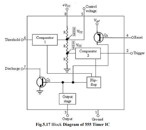
From
the above figure, three 5k internal resistors act as voltage divider providing
bias voltage of 2/3 Vcc to the upper comparator & 1/3 Vcc to the lower
comparator. It is possible to vary time
electronically by applying a modulation voltage to the control voltage input
terminal (5).
(i)
In the Stable state:
The
output of the control FF is high. This means that the output is low because of
power amplifier which is basically an inverter. Q = 1; Output = 0
(ii)
At the Negative going trigger pulse:
The
trigger passes through (Vcc/3) the output of the lower comparator goes high
& sets the FF. Q = 1; Q = 0
(iii) At the Positive going trigger pulse:
It
passes through 2/3Vcc, the output of the upper comparator goes high and resets
the FF. Q = 0; Q = 1
The
reset input (pin 4) provides a mechanism to reset the FF in a manner which
overrides the effect of any instruction coming to FF from lower comparator.
Monostable Operation:
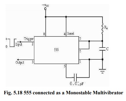
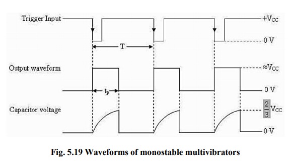
Initially
when the output is low, i.e. the circuit is in a stable state, transistor Q1 is
ON & capacitor C is shorted to ground. The output remains low. During
negative going trigger pulse, transistor Q1 is OFF, which releases the short
circuit across the external capacitor C & drives the output high. Now the
capacitor C starts charging toward Vcc through RA. When the voltage across the
capacitor equals 2/3 Vcc, upper comparator switches from low to high. i.e. Q =
0, the transistor Q1 = OFF ; the output is high.
Since
C is unclamped, voltage across it rises exponentially through R towards Vcc
with a time constant RC (fig b) as shown in below. After the time period,
the upper comparator resets the FF, i.e. Q = 1, Q1 = ON; the output is
low.[i.e discharging the capacitor C to ground potential (fig c)]. The voltage
across the capacitor as in fig (b) is given by
Vc
= Vcc (1-e-t/RC)……. (1)
Therefore
At t = T, Vc = 2/3 Vcc
2/3
Vcc = Vcc(1-e-T/RC)
or
T = RC ln (1/3)
Or
T = 1.1RC seconds ……………. (2)
If the reset is applied Q2 = OFF, Q1 = ON, timing capacitor C immediately discharged. The output now will be as in figure (d & e). If the reset is released output will still remain low until a negative going trigger pulse is again applied at pin 2.
Applications of Monostable Mode of Operation:
(a) Frequency Divider:
The
555 timer as a monostable mode. It can be used as a frequency divider by
adjusting the length of the timing cycle tp with respect to the time period T
of the trigger input. To use the monostable multivibrator as a divide by 2
circuit, the timing interval tp must be a larger than the time period of the
trigger input. [Divide by 2, tp > T
of the trigger]
By
the same concept, to use the monostable multivibrator as a divide by 3 circuit,
tp must be slightly larger than twice the period of the input trigger signal
& so on, [ divide by 3 tp > 2T oftrigger]
(b) Pulse width modulation:
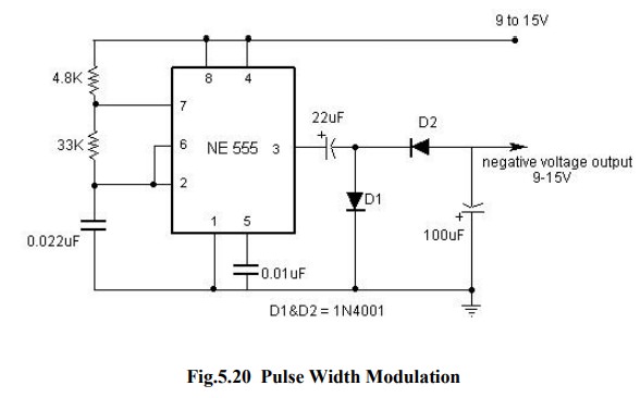
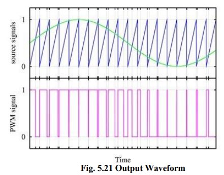
Pulse
width of a carrier wave changes in accordance with the value of a incoming
(modulating signal) is known as PWM. It is basically monostable multivibrator.
A
modulating
signal is fed in to the control voltage (pin 5). Internally, the control
voltage is adjusted to 2/3 Vcc externally applied modulating signal changes the
control voltage level of upper comparator. As a result, the required to change
the capacitor up to threshold voltage level changes, giving PWM output.
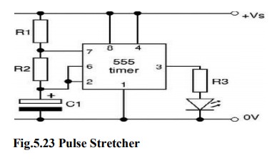
(c) Pulse Stretcher:
This
application makes use of the fact that the output pulse width (timing interval)
of the monostable multivibrator is of longer duration than the negative pulse
width of the input trigger. As such, the output pulse width of the monostable
multivibrator can be viewed as a stretched version of the narrow input pulse,
hence the name “Pulse stretcher”.
Often,
narrow –pulse width signals are not suitable for driving an LED display, mainly
because of their very narrow pulse widths. In other words, the LED may be
flashing but not be visible to the eye because its on time is infinitesimally
small compared to its off time. The 55 pulse stretcher can be used to remedy
this problem. The LED will be ON during the timing interval tp = 1.1RAC which
can be varied by changing the value of RA & C.
The 555 timer as an Astable Multivibrator:
An
Astable multivibrator, often called a free running multivibrator, is a
rectangular wave generating circuit. Unlike the monostable multivibrator, this
circuit does not require an external trigger to change the state of the output,
hence the name free running. However, the time during which the output is
either high or low is determined by 2 resistors and capacitors, which are
externally connected to the 55 timer.
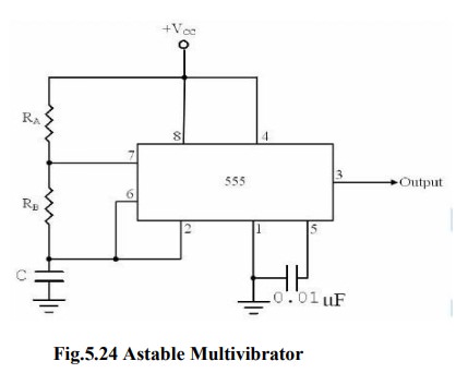
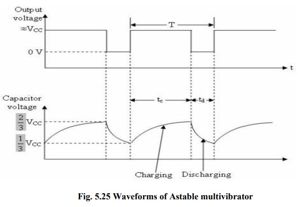
The
above figures show the 555 timer connected as an astable multivibrator and its
model graph
Initially, when the output is high :
Capacitor
C starts charging toward Vcc through RA & RB. However, as soon as voltage
across the capacitor equals 2/3 Vcc. Upper comparator triggers the FF &
output switches low.
When the output becomes Low:
Capacitor
C starts discharging through RB and transistor Q1, when the voltage across C
equals 1/3 Vcc, lower comparator output triggers the FF & the output goes
high. Then cycle repeats. The capacitor is periodically charged &
discharged between 2/3 Vcc & 1/3 Vcc respectively. The time during which
the capacitor charges from 1/3 Vcc to 2/3 Vcc equal to the time the output is
high & is given by
tc
= (RA+RB)C ln 2……………(1) Where [ln 2 = 0.69]
=
0.69 (RA+RB) C
Where
RA & RB are in ohms. And C is in
farads.
Similarly,
the time during which the capacitors discharges from 2/3 Vcc to 1/3 Vcc is
equal to the time, the output is low and is given by,
tc
= RB C ln 2
td
= 0.69 RB C …………………..(2)
where
RB is in ohms and C is in farads.
Thus
the total period of the output waveform is
T
= tc + td = 0.69
(RA+2RB) C …………….(3)
This,
in turn, gives the frequency of oscillation as,f 0 = 1/T =
1.45/(RA+2RB)C ………(4)
Equation
4 indicates that the frequency f 0 is independent of the supply voltage Vcc.
Often the term duty cycle is used in conjunction with the astable
multivibrator. The duty cycle is the ratio of the time tc during which the
output is high to the total time period T. It is generally expressed as a
percentage.
% duty cycle = (tc / T )* 100
% DC = [(RA+RB)/ /(RA+2RB)] * 100
Astable Multivibrator Applications:
(a) Square wave oscillator:
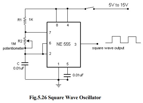
Without
reducing RA = 0 ohm, the astable multivibrator can be used to produce square wave output. Simply by connecting diode D
across Resistor RB. The capacitor C charges through RA & diode D to
approximately 2/3Vcc & discharges through RB & Q1 until the capacitor
voltage equals approximately 1/3Vcc, then the cycle repeats.
To
obtain a square wave output, RA must be a combination of a fixed resistor &
potentiometer so that the potentiometer can be adjusted for the exact square
wave.
(b) Free – running Ramp generator:
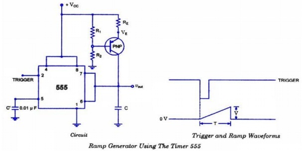
·
The
astable multivibrator can be used as a free – running ramp generator when
resistor
·
RA
& RB is replaced by a current mirror.
·
The
current mirror starts charging capacitor C toward Vcc at a constant rate.
·
When
voltage across C equals to 2/3 Vcc,
upper comparator turns transistor Q1 ON and C rapidly discharges
through transistor Q1.
·
When
voltage across C equals to 1/3 Vcc,
lower comparator switches transistor OFF & then capacitor C starts charging
up again.
·
Thus
the charge – discharge cycle keeps repeating.
·
The
discharging time of the capacitor is relatively negligible compared to its
charging time.
·
The
time period of the ramp waveform is equal to the charging time & is
approximately is given by,
T
= VccC/3IC
IC
= (Vcc - VBE)/R = constant current
Therefore
the free – running frequency of ramp generator is
f0
= 3IC/ Vcc C
Related Topics