Chapter: Linear Integrated Circuits : Waveform Generators and Special Function ICs
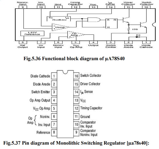
Monolithic Switching Regulator [┬Ąa78s40]
Monolithic
Switching Regulator [┬Ąa78s40]:
The
┬ĄA78S40 consists of a temperature compensated voltage reference, duty cycle
controllable oscillator with an active current limit circuit, a high gain
comparator, a high- current, high voltage output switch, a power switching
diode & an uncommitted op-amp. Important features of the ┬ĄA78S40 switching
regulators are:
┬Ę
Step
up, down & Inverting operation
┬Ę
Operation
from 2.5 to 40V input
┬Ę
80dB
line & load regulations
┬Ę
Output
adjustable from 1.3 to 40V
┬Ę
Peak
current to 1.5A without external resistors
┬Ę
Variable
frequency, variable duty cycle device
The
internal switching frequency is set by the timing capacitor CT, connected
between pin12 & ground pin 11. The initial duty cycle is 6:1. The switching
frequency & duty cycle can be modified by the current limit circuitry, IPK
sense, pin14, 7 the comparator, pin9 & 10.
Comparator:
The
comparator modifies the OFF time of the output switch transistor Q1 & Q2.
In the step ŌĆō up & step down modes, the non-inverting input(pin9) of the
comparator is connected to the voltage reference of 1.3V (pin8) & the
inverting input (pin10) is connected to the output terminal via the voltage
divider network.
┬Ę
In the
Inverting mode the non ŌĆō inverting input is connected to both the voltage
reference & the output terminal through 2 resistors & the inverting
terminal is connected to ground.
┬Ę
When the
output voltage is correct, the comparator output is in high state & has no
effect on the circuit operation.
┬Ę
However,
if the output is too high & the voltage at the inverting terminal is higher
than that at the non-inverting terminal, then the comparator output goes low.
┬Ę
In
the LOW state the comparator inhibits the turn on of the output switching
transistors. This means that, as long as the comparator output is low, the
system is in off time.
┬Ę
As
the output current rises or the output voltage falls, the off time of the
system decreases.
┬Ę
Consequently,
as the output current nears its maximum IoMAX, the off time approaches its
minimum value.
In
all 3 modes (Step down, step up, Inverting), the current limit circuit is
completed by connecting a sense resistor Rsc, between IPK sense & Vcc.
┬Ę
The
current limit circuit is activated when a 330mV potential appears across Rsc.
┬Ę Rsc is selected such that 330mV appears across it when the desired peak current IPK, flows through it.
┬Ę
When
the peak current is reached, the current limit circuit is turned on.
The
forward voltage drop, VD, across the internal power diode is used to determine
the value of inductor L off time & efficiency of the switching regulator.
Another
important quantity used in the design of a switching regulator is the
saturation voltage Vs:
In
the step down mode an ŌĆ£output saturation voltŌĆØ is 1.1V typical, 1.3VMAX.
In
the step up mode an ŌĆ£Output saturation voltŌĆØ is 0.45V typical, 0.7 maximum.
The
desired peak current value is reached; the current limiting circuit turns ON
& immediately terminates the ON time & starts OFF time.
┬Ę
As
we increase IL (load current), Vout will decrease, to compensate for this, the
ON time of the output is increased automatically.
If
the IL decreased then Vout increased, to compensate for this, the OFF time of
the output is increased automatically.
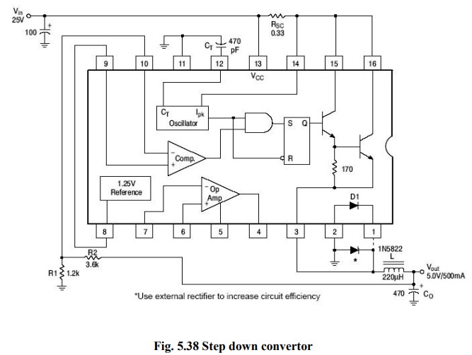
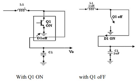
(i)
Step ŌĆō Down Switching Regulator:
┬Ę
CT
is the timing capacitor which decides the switching frequency. ’éĘ Rsc is the current sensing resistance. Its value is given
by
┬Ę
The
Non-inverting terminal of the internal op-amp (pin9) is connected to the 1.3V
reference (pin8).
┬Ę
Resistances
R1 & R2 from a potential divider, across the output voltage Vo. Their value
should be such that the potential at the inverting input of the op-amp should
be equal to 1.3V ref when Vo is at its desired level.
The
output capacitance Co is used for reducing the ripple contents in the output
voltage. It acts as a filter along with the inductor L.
┬Ę
The
inductor L is a part of filter connected on the output side, to reduce the
ripple percentage.
┬Ę
The
0.1╬╝F capacitor connected between pin8 & ground bypasses any noise voltage
coupled to the reference (pin8).
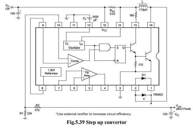
(ii)
Step ŌĆō Up Switching Regulator:
┬Ę
Inductor
is connected between the collectors of Q1 & Q2.
┬Ę
When
Q1 is ON, the output is shorted & the collector current of Q1 flows through
L.
┬Ę
The
diode D1 is reverse biased & Co supplies the load current.
┬Ę
The
inductor stores the energy. When the Q1 is turned OFF, there is a self induced
emf that appears across the inductor with polarities.
┬Ę
The
output voltage is given by,
Vo
= Vin + VL
┬Ę
Hence
it will be always higher than Vin & step up operation is achieved.
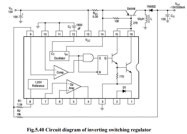
(iii) Inverting
Switching Regulator:
Inverting
switching regulator converts a positive input voltage into a negative output
voltage which is higher in magnitude.
Related Topics