Disadvantages, Features, Functional block diagram - IC 723 - General Purpose Regulator | Linear Integrated Circuits : Waveform Generators and Special Function ICs
Chapter: Linear Integrated Circuits : Waveform Generators and Special Function ICs
IC 723 - General Purpose Regulator
IC 723 –
General Purpose Regulator
Disadvantages of fixed voltage regulator:
1.
Do
not have the shot circuit
2.
Output
voltage is not adjustable
These
limitations can be overcomes in IC723.
Features of IC723:
1.
Unregulated
dc supply voltage at the input between 9.5V & 40V
2.
Adjustable
regulated output voltage between 2 to 3V.
3.
Maximum
load current of 150 mA (ILmax = 150mA).
4.
With
the additional transistor used, ILmax upto 10A is obtainable.
5.
Positive
or Negative supply operation
6.
Internal
Power dissipation of 800mW.
7.
Built
in short circuit protection.
8.
Very
low temperature drift.
9.
High
ripple rejection.
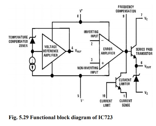
The simplified functional block diagram can be divided in to 4 blocks.
1.
Reference
Generating block:
The
temperature compensated Zener diode, constant current source & voltage
reference amplifier together from the reference generating block. The Zener
diode is used to generate a fixed reference voltage internally. Constant
current source will make the Zener diode to operate at affixed point & it
is applied to the Non – inverting terminal of error amplifier. The Unregulated
input voltage ±Vcc is applied to the voltage reference amplifier as well as
error amplifier.
2. Error Amplifier:
Error amplifier is a high gain differential amplifier with 2 input (inverting & Non-inverting). The Non-inverting terminal is connected to the internally generated reference voltage. The Inverting terminal is connected to the full regulated output voltage.
3.
Series
Pass Transistor:
Q1
is the internal series pass transistor which is driven by the error amplifier.
This transistor actually acts as a variable resistor & regulates the output
voltage. The collector of transistor Q1 is connected to the Un-regulated power
supply. The maximum collector voltage of Q1 is limited to 36Volts. The maximum
current which can be supplied by Q1 is 150mA.
4.
Circuitry
to limit the current:
The
internal transistor Q2 is used for current sensing & limiting. Q2 is
normally OFF transistor. It turns ON when the IL exceeds a predetermined limit.
Low
voltage, Low current is capable of supplying load voltage which is equal to or
between 2 to 7Volts.
Vload
= 2 to 7V and Iload= 50mA
IC723 as a LOW voltage LOW current:
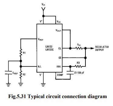
·
R1
& R2 from a potential divider between Vref & Gnd.
·
The
Voltage across R2 is connected to the Non – inverting terminal of
the regulator IC Vnon-inv = R2/(R1+R2)
Vref
·
Gain
of the internal error amplifier is large
Vnon-inv
= Vin
·
Therefore
the Vo is connected to the Inverting terminal through R3 & RSC
must also be equal to Vnon-inv
Vo
= Vnon-inv =R2/(R1+R2)
Vref
R1
& R2 can be in the range of 1 KΩ to 10KΩ & value of R3 is
given by
R3
= R1ll R2 =R1R2/(R1+R2)
Rsc
(current sensing resistor) is connected between Cs & CL. The voltage drop
across Rsc is proportional to the IL.
·
This
resistor supplies the output voltage in the range of 2 to 7 volts, but the load
current can be higher than 150mA.
·
The
current sourcing capacity is increased by including a transistor Q in the
circuit.
·
The
output voltage , Vo =R2/(R1+R2)
Vref
IC723 as a HIGH voltage LOW Current:
·
This
circuit is capable of supplying a regulated output voltage between the ranges
of 7 to 37 volts with a maximum load current of 150 mA.
·
The
Non – inverting terminal is now connected to Vref through resistance
R3.
·
The
value of R1 & R2 is adjusted in order to get a
voltage of Vref at the inverting terminal at the desired output.
Vin
= Vref =R2 /(R1+R2)V0
Vo
= [1+R1/R2] Vin
·
Rsc
is connected between CL & Cs terminals as before & it provides the
short Circuit current limiting Rsc =0.6/Ilimit
·
The
value of resistors R3 is given by ,
R3= R1ll R2
=R1R2/(R1+R2)
IC723 as a HIGH voltage HIGH Current:
·
An
external transistor Q is added in the circuit for high voltage low current
regulator to improve its current sourcing capacity.
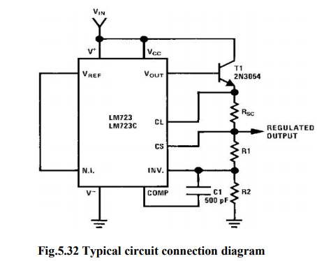
·
For
this circuit the output voltage varies between 7 & 37V.
·
Transistor
Q increase the current sourcing capacity thus IL (MAX) is greater than 150mA.
·
The
output voltage Vo is given by ,
V0=
Vo = [1+R1/R2] Vin
Rsc
=0.6/Ilimit
Related Topics