Chapter: Linear Integrated Ciruits : IC Fabrication and Circuit Configuration for Linear ICs
Schottky Barrier Diode

Schottky Barrier Diode:
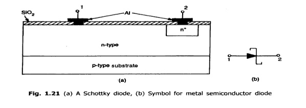
The metal
contacts are required to be ohmic and no PN junctions to be formed between the
metal and silicon layers. The N+ diffusion region serves the purpose
of generating ohmic contacts. On the other hand, if aluminium is deposited
directly on the N-type silicon, then a metal semiconductor diode can be said to
be formed. Such a metal semiconductor diode junction exhibits the same type of
V-I Characteristics as that of an ordinary PN junction.
The cross
sectional view and symbol of a Schottky barrier diode as shown in figure.
Contact 1 shown in figure is a Schottky barrier and the contact 2 is an ohmic
contact. The contact potential between the semiconductor and the metal
generated a barrier for the flow of conducting electrons from semiconductor to
metal. When the junction is forward biased this barrier is lowered and the
electron flow is allowed from semiconductor to metal, where the electrons are
in large quantities.

The
minority carriers carry the conduction current in the Schottky diode whereas in
the PN junction diode, minority carriers carry the conduction current and it
incurs an appreciable time delay from ON state to OFF state. This is due to the
fact that the minority carriers stored in the junction have to be totally
removed. This characteristic puts the Schottky barrier diode at an advantage
since it exhibits negligible time to flow the electron from N-type silicon into
aluminum almost right at the contact surface, where they mix with the free
electrons. The other advantage of this diode is that it has less forward
voltage (approximately 0.4V). Thus it can be used for clamping and detection in
high frequency applications and microwave integrated circuits.
Related Topics