Chapter: Linear Integrated Ciruits : IC Fabrication and Circuit Configuration for Linear ICs
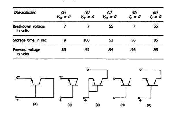
Monolithic diodes
Monolithic diodes:
The diode
used in integrated circuits are made using transistor structures in one of the
five possible connections. The three most popular structures are shown in
figure. The diode is obtained from a transistor structure using one of the
following structures.
1.
The emitter-base diode, with collector short
circuited to the base.
2.
The emitter-base diode with the collector open and
3.
The collector –base diode, with the emitter
open-circuited.
The
choice of the diode structure depends on the performance and application
desired. Collector-base diodes have higher collector-base arrays breaking
rating, and they are suitable for common-cathode diode arrays diffused within a
single isolation island. The emitter-base diffusion is very popular for the
fabrication of diodes, provided the reverse-voltage requirement of the circuit
does not exceed the lower base-emitter breakdown voltage.
1. Integrated Resistors:
A
resistor in a monolithic integrated circuit is obtained by utilizing the bulk
resistivity of the diffused volume of semiconductor region. The commonly used
methods for fabricating integrated resistors are 1. Diffused 2.epitaxial 3.
Pinched and 4. Thin film techniques.
2. Diffused Resistor:
The
diffused resistor is formed in any one of the isolated regions of epitaxial
layer during base or emitter diffusion processes. This type of resistor
fabrication is very economical as it runs in parallel to the bipolar transistor
fabrication. The N-type emitter diffusion and P-type base diffusion are
commonly used to realize the monolithic resistor.
The
diffused resistor has a severe limitation in that, only small valued resistors
can be fabricated. The surface geometry such as the length, width and the
diffused impurity profile determine the resistance value. The commonly used
parameter for defining this resistance is called the sheet resistance. It is
defined as the resistance in ohms/square offered by the diffused area.
In the monolithic resistor, the resistance value is expressed by R = Rs 1/w
where R=
resistance offered (in ohms)
Rs =
sheet resistance of the particular fabrication process involved (in
ohms/square)
l =
length of the diffused area and w = width of the diffused area.
The sheet
resistance of the base and emitter diffusion in 200Ω/Square and 2.2Ω/square
respectively. For example, an emitter-diffused strip of 2mil wide and 20 mil
long will offer a resistance of 22Ω. For higher values of resistance, the
diffusion region can be formed in a zig-zag fashion resulting in larger
effective length. The poly silicon layer can also be used for resistor
realization.
3.
Epitaxial Resistor:
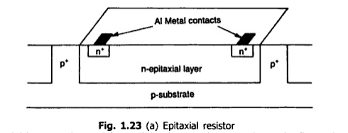
The
N-epitaxial layer can be used for realizing large resistance values. The figure
shows the cross-sectional view of the epitaxial resistor formed in the
epitaxial layer between the two N+aluminium metal contacts.
4.
Pinched resistor:
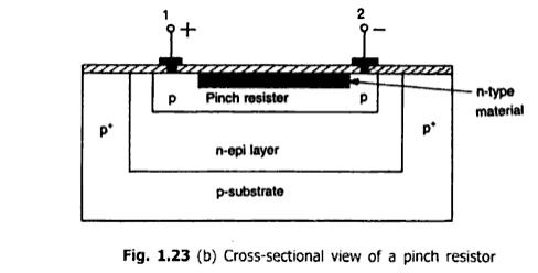
The sheet
resistance offered by the diffusion regions can be increased by narrowing down
its cross-sectional area. This type of resistance is normally achieved in the
base region. Figure shows a pinched base diffused resistor. It can offer
resistance of the order of mega ohms in a comparatively smaller area. In the
structure shown, no current can flow in the N-type material
since the
diode realized at contact 2 is biased in reversed direction. Only very small
reverse saturation current can flow in conduction path for the current has been
reduced or pinched. Therefore, the resistance between the contact 1 and 2
increases as the width narrows down and hence it acts as a pinched resistor.
5. Thin
film resistor:
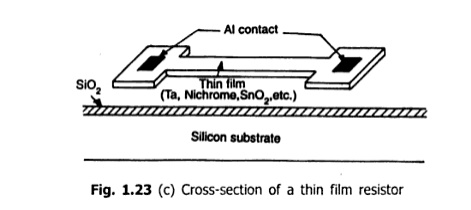
The thin
film deposition technique can also be used for the fabrication of monolithic
resistors. A very thin metallic film of thickness less than 1μm is deposited on
the silicon dioxide layer by vapour deposition techniques. Normally, Nichrome
(NiCr) is used for this process. Desired geometry is achieved using masked etching
processes to obtain suitable value of resistors. Ohmic contacts are made using
aluminium metallization as discussed in earlier sections.
The
cross-sectional view of a thin film resistor as shown in figure. Sheet
resistances of 40 to 400Ω/ square can be easily obtained in this method and
thus 20kΩ to 50kΩ values are very practical.
The
advantages of thin film resistors are as follows:
1.
They have smaller parasitic components which makes
their high frequency behaviour good.
2.
The thin film resistor values can be very minutely
controlled using laser trimming.
3.
They have low temperature coefficient of resistance
and this makes them more stable.
The thin
film resistor can be obtained by the use of tantalum deposited over silicon
dioxide layer. The main disadvantage of thin film resistor is that its
fabrication requires additional processing steps.
Related Topics