Chapter: Linear Integrated Ciruits : IC Fabrication and Circuit Configuration for Linear ICs
Construction of a Monolithic Bipolar Transistor
Construction of a Monolithic
Bipolar Transistor:
The
fabrication of a monolithic transistor includes the following steps.
1.
Epitaxial growth
2.
Oxidation
3.
Photolithography
4.
Isolation diffusion
5.
Base diffusion
6.
Emitter diffusion
7.
Contact mask
8.
Aluminium metallization
9.
Passivation
The
letters P and N in the figures refer to type of doping, and a minus (-) or plus
(+) with P and N indicates lighter or heavier doping respectively.
1. Epitaxial growth:
The first
step in transistor fabrication is creation of the collector region. We normally
require a low resistivity path for the collector current. This is due to the
fact that, the collector contact is normally taken at the top, thus increasing
the collector series resistance and the VCE(Sat) of the device.
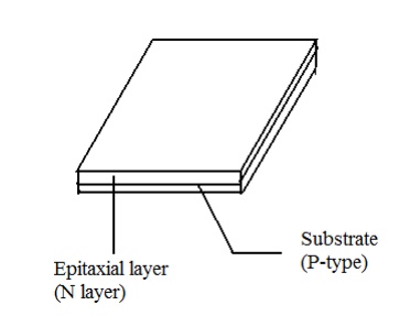
The
higher collector resistance is reduced by a process called buried layer as
shown in figure. In this arrangement, a heavily doped ‗N‘ region is sandwiched
between the N-type epitaxial layer and P – type substrate. This buried N+
layer provides a low resistance path in the active collector
region to
the collector contact C. In effect, the buried layer provides a low resistance
shunt path for the flow of current.
For
fabricating an NPN transistor, we begin with a P-type silicon substrate having
a resistivity of typically 1Ω-cm, corresponding to an acceptor ion
concentration of 1.4 * 1015 atoms/cm3 . An oxide mask
with the necessary pattern for buried layer diffusion is prepared. This is
followed by masking and etching the oxide in the buried layer mask.
The
N-type buried layer is now diffused into the substrate. A slow-diffusing
material such as arsenic or antimony us used, so that the buried layer will
stay-put during subsequent diffusions. The junction depth is typically a few
microns, with sheet resistivity of around 20Ω per square.
Then, an
epitaxial layer of lightly doped N-silicon is grown on the P-type substrate by
placing the wafer in the furnace at 12000 C and introducing a gas
containing phosphorus (donor impurity). The resulting structure is shown in
figure.
The
subsequent diffusions are done in this epitaxial layer. All active and passive
components are formed on the thin N-layer epitaxial layer grown over the P-type
substrate. Obtaining an epitaxial layer of the proper thickness and doping with
high crystal quality is perhaps the most formidable challenge in bipolar device
processing.
2. Oxidation:
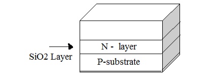
As shown in figure, a thin layer of silicon dioxide (SiO2) is grown over the N-type layer by exposing the silicon wafer to an oxygen atmosphere at about 10000 C.
3. Photolithography:
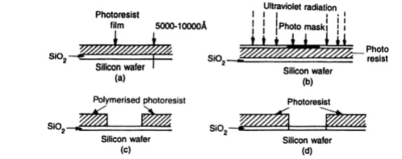
The prime
use of photolithography in IC manufacturing is to selectively etch or remove
the SiO2 layer. As shown in figure, the surface of the oxide is first covered
with a thin uniform layer of photosensitive emulsion (Photo resist). The mask,
a black and white negative of the requied pattern, is placed over the
structure. When exposed to ultraviolet light, the photo resist under the
transparent region of the mask becomes poly-merized. The mask is then removed
and the wafer is treated chemically that removes the unexposed portions of the
photoresist film. The polymerized region is cured so that it becomes resistant
to corrosion. Then the chip is dipped in an etching solution of hydrofluoric
acid which removes the oxide layer not protected by the polymerized
photoresist. This creates openings in the SiO2 layer through which P-type or
N-type impurities can be diffused using the isolation diffusion process as
shown in figure. After diffusion of impurities, the polymerized photoresist is
removed with sulphuric acid and by a mechanical abrasion process.
4. Isolation Diffusion:
The
integrated circuit contains many devices. Since a number of devices are to be
fabricated on the same IC chip, it becomes necessary to provide good isolation
between various components and their interconnections.
The most
important techniques for isolation are:
1.
PN junction Isolation
2.
Dielectric Isolation
In PN
junction isolation technique, the P+ type impurities are selectively
diffused into the N-type epitaxial layer so that it touches the P-type
substrate at the bottom. This method generated N-type isolation regions
surrounded by P-type moats. If the P-substrate is held at the most negative
potential, the diodes will become reverse-biased, thus providing isolation
between these islands.
The
individual components are fabricated inside these islands. This method is very
economical, and is the most commonly used isolation method for general purpose
integrated circuits.
In
dielectric isolation method, a layer of solid dielectric such as silicon
dioxide or ruby surrounds each component and this dielectric provides
isolation. The isolation is both physical and electrical. This method is very
expensive due to additional processing steps needed and this is mostly used for
fabricating IC‘s required for special application in military and aerospace.
The PN
junction isolation diffusion method is shown in figure. The process take place
in a furnace using boron source. The diffusion depth must be atleast equal to
the epitaxial thickness in order to obtain complete isolation. Poor isolation
results in device failures as all transistors might get shorted together. The
N-type island shown in figure forms the collector region of the NPN transistor.
The heavily doped P-type regions marked P+ are the isolation regions
for the active and passive components that will be formed in the various N-type
islands of the epitaxial layer.
5 Base diffusion:
Formation
of the base is a critical step in the construction of a bipolar transistor. The
base must be aligned, so that, during diffusion, it does not come into contact
with either the isolation region or the buried layer. Frequently, the base
diffusion step is also used in parallel to fabricate diffused resistors for the
circuit. The value of these resistors depends on the diffusion conditions and
the width of the opening made during etching. The base width influences the
transistor parameters very strongly. Therefore, the base junction depth and
resistivity must be tightly controlled. The base sheet resistivity should be
fairly high (200- 500Ω per square) so that the base does not inject carriers
into the emitter. For NPN transistor, the base is diffused in a furnace using a
boron source. The diffusion process is done in two steps, pre deposition of
dopants at 9000 C and driving them in at about 12000 C.
The drive-in is done in an oxidizing ambience, so that oxide is grown over the
base region for subsequent fabrication steps. Figure shows that P-type base
region of the transistor diffused in the N-type island (collector region) using
photolithography and isolation diffusion processes.
6. Emitter Diffusion:
Emitter
Diffusion is the final step in the fabrication of the transistor. The emitter
opening must lie wholly within the base. Emitter masking not only opens windows
for the emitter, but also for the contact point, which provides a low
resistivity ohmic contact path for the emitter terminal.
The
emitter diffusion is normally a heavy N-type diffusion, producing
low-resistivity layer that can inject charge easily into the base. A Phosphorus
source is commonly used so that the diffusion time id shortened and the
previous layers do not diffuse further. The emitter is diffused into the base,
so that the emitter junction depth very closely approaches the base junction
depth. The active base is then a P-region between these two junctions which can
be made very narrow by adjusting the emitter diffusion time. Various diffusion
and drive in cycles can be used to fabricate the emitter. The Resistivity of
the emitter is usually not too critical.
The
N-type emitter region of the transistor diffused into the P-type base region is
shown below. However, this is not needed to fabricate a resistor where the
resistivity of the P-type base region itself will serve the purpose. In this
way, an NPN transistor and a resistor are fabricated simultaneously.
7. Contact Mask:
After the
fabrication of emitter, windows are etched into the N-type regions where
contacts are to be made for collector and emitter terminals. Heavily
concentrated phosphorus N+ dopant is diffused into these regions
simultaneously.
The
reasons for the use of heavy N+ diffusion is explained as follows:
Aluminium, being a good conductor used for interconnection, is a P-type of
impurity when used with silicon. Therefore, it can produce an unwanted diode or
rectifying contact with the lightly doped N-material. Introducing a high
concentration of N+ dopant caused the Si lattice at the surface
semi-metallic. Thus the N+ layer makes a very good ohmic contact
with the Aluminium layer. This is done by the oxidation, photolithography and
isolation diffusion processes.
8. Metallization:
The IC
chip is now complete with the active and passive devices, and the metal leads
are to be formed for making connections with the terminals of the devices.
Aluminium is deposited over the entire wafer by vacuum deposition. The
thickness for single layer metal is 1μ m. Metallization is carried out by
evaporating aluminium over the entire surface and then selectively etching away
aluminium to leave behind the desired interconnection and bonding pads as shown
in figure.
Metallization
is done for making interconnection between the various components fabricated in
an IC and providing bonding pads around the circumference of the IC chip for
later connection of wires
9. Passivation/ Assembly and Packaging:
Metallization
is followed by passivation, in which an insulating and protective layer is
deposited over the whole device. This protects it against mechanical and
chemical damage during subsequent processing steps. Doped or undoped silicon
oxide or silicon nitride, or some combination of them, are usually chosen for
passivation of layers. The layer is deposited by chemical vapour deposition
(CVD) technique at a temperature low enough not to harm the metallization.
Related Topics