Chapter: Electronic Circuits : Biasing of Discrete BJT and MOSFET
FET Biasing
FET Biasing
The
Parameters of FET is temperature dependent .When temperature increases drain
resistance also increases, thus reducing the drain current.
Unlike
BJTs, thermal runaway does not occur with FETs
However,
the wide differences in maximum and minimum transfer characteristics make ID
levels unpredictable with simple fixed-gate bias voltage.
Different
biasing circuits of FET are
1.
Fixed bias circuits
2.
Self bias circuits
3.
Voltage bias circuits
Fixed bias circuits
DC bias
of a FET device needs setting of gate-source voltage VGS to give
desired drain current ID . For a JFET drain current is limited by
the saturation current IDS. Since the FET has such a high input
impedance that no gate current flows and the dc voltage of the gate set by a
voltage divider or a fixed battery voltage is not affected or loaded by the
FET.

Fixed dc
bias is obtained using a battery VQG. This battery ensures that the
gate is always negative with respect to source and no current flows through
resistor RG and gate terminal that is IG =0. The battery
provides a voltage VGS to bias the N-channel JFET, but no resulting
current is drawn from the battery VGG. Resistor RG is
included to allow any ac signal applied through capacitor C to develop across RG.
While any ac signal will develop across RG, the dc voltage drop
across RG is equal to IG RGi.e. 0 volt.
Calculate VGS
For DC
analysis IG =0., applying KVL to the input circuits
VGS+
VGG=0
VGS=
- VGG
As VGS
is a fixed dc supply, hence the name fixed bias circuit
Calculate IDQ
IDQ=IDss(1-
VGS/VGp)2
Calculate VDS
This
current IDQ then causes a voltage drop across the drain resistor RD
and is given as
VDSQ
= VDD – ID RD
Disadvantage
The fixed
bias circuit of FET requires two power supplies.
Self-Bias circuits
Self-Bias
circuits is the most common method for biasing a JFET. Self-bias circuit for
N-channel JFET is shown in figure
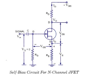
The gate
source junction of JFET must be always in reverse biased condition .No gate
current flows through the reverse-biased gate-source, the gate current IG
= 0 and, therefore,vG = iG RG = 0
With a drain
current ID the voltage
at the S is
Vs=
IDRs
1)The
gate-source voltage is then
VGS
= VG - Vs = 0 – ID RS = – ID
RS
So
voltage drop across resistance Rs provides the biasing voltage VGg
and no external source is required for biasing and this is the reason that it
is called self-biasing. 2)Calculate IDQ
ID=IDSS(1-
VGS/ VP)2
Substituting
the value of VGS
ID=
IDSS (1+IDRS
/ VP)2
3)The
operating point (that is zero signal
ID and VDS) can easily be determined from equation given
below :
VDS
= VDD – ID(RD
+ RS)
Self
biasing of a JFET stabilizes its quiescent operating point against any change
in its parameters like transconductance. Any increase in voltage drop across RS,
therefore, gate-source voltage, VGS becomes more negative and thus
increase in drain current is reduced.
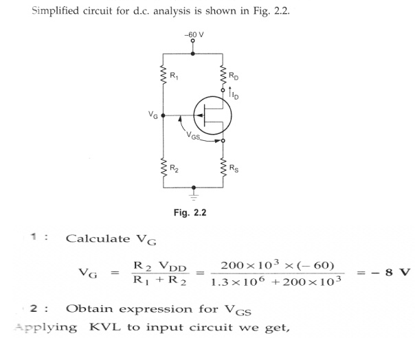
Voltage -Divider Bias circuits
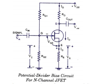
The
resistors RGl and RG2 form a potential divider across
drain supply VDD. The voltage V2 across RG2
provides the necessary bias. The additional gate resistor RGl from
gate to supply voltage facilitates in larger adjustment of the dc bias point
and permits use of larger valued RS.
The
coupling capacitors are assumed to be open circuit for DC analysis
1) The
gate is reverse biased so that IG = 0 and gate voltage
VG
=V2 = (VDD/R G1 + R G2 ) *RG2
2) Applying
KVL to the input circuit we get
VGS= VG – VS = VG
- ID RS
3) IDQ=
IDSS(1- VGS/ VP)2
4) VDS
= VDD – ID (RD + RS)
The
operating point of a JFET amplifier using the Voltage -Divider Bias is
determined by
IDQ=
IDSS(1- VGS/ VP)2
VDSQ
= VDD – ID (RD + RS)
VGSQ
= VG – ID RS
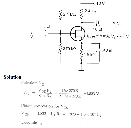
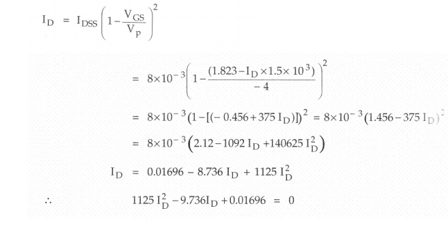
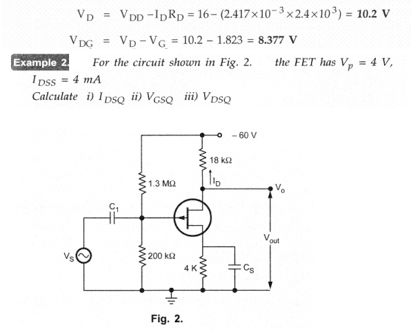
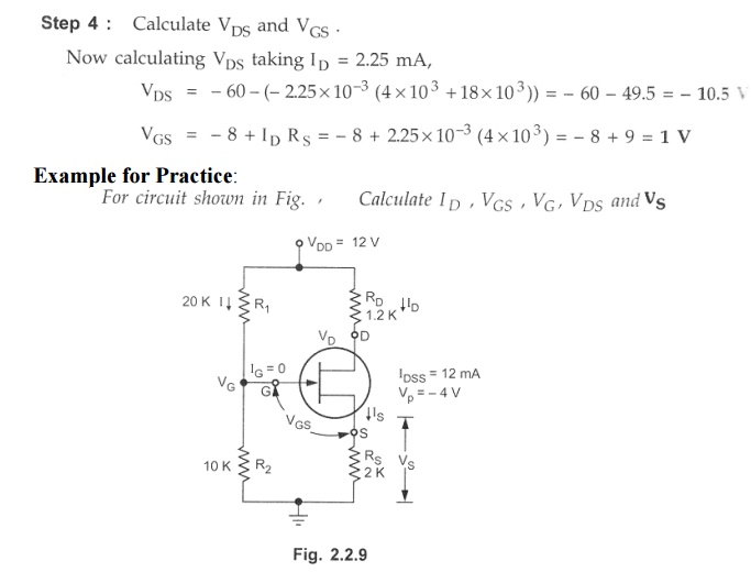
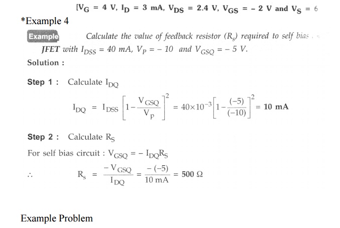
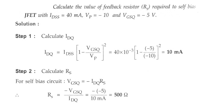
Example Problems
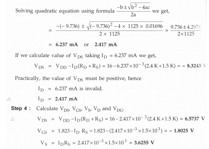
1)Determine
IDQ, VGSQ, VD, VS, VDS,
and VDG
Related Topics