Chapter: Electronic Circuits : Biasing of Discrete BJT and MOSFET
Collector to Base Bias
Collector to Base Bias
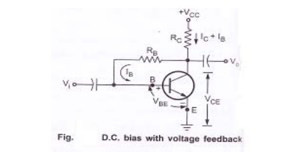
Figure
shows the dc bias with voltage feedback. It is also called as collector to base
bias circuit. It is an improvement over fixed bias method. In this, biasing
resistor is connected between collector and base of the transistor to provide
feedback path.
Circuit analysis:
Base circuit:
Consider
the base circuit and applying voltage law then we get,
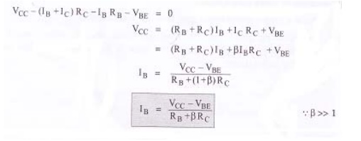
Only the
difference between the equation for IB and that obtained for fixed
bias configuration is βRC, so the feedback path results in a
reflection of the resistance RC to the input circuit.
Collector circuit:
Applying
KVL to the collector circuit,
VCC
– (IC + IB) RC – VCE = 0
VCE
= VCC – (IC + IB) RC
If there
is a change in β due to piece to piece variation between transistors or if
there is a change in β and I CO due to the change in temperature. So
collector current tends to increase. As a result, voltage drop across RC
increases. Due to reduction in VCE, IB reduces. The
result is that the circuit tends to maintain a stable value of collector
current, keeping the Q point fixed.
In this
circuit, RB appears directly across input and output. A part of
output is feedback to the input. And increase in collector current decreases
the base current. So negative feedback exists in the circuit. It is also called
as voltage feedback bias circuit.
Related Topics