Chapter: Distributed and Cloud Computing: From Parallel Processing to the Internet of Things : Computer Clusters for Scalable Parallel Computing
Computer Clusters and MPP Architectures
COMPUTER CLUSTERS AND MPP ARCHITECTURES
Most clusters emphasize higher availability and
scalable performance. Clustered systems evolved from the Microsoft Wolfpack and
Berkeley NOW to the SGI Altix Series, IBM SP Series, and IBM Roadrunner. NOW
was a UC Berkeley research project designed to explore new mechanisms for
clustering of UNIX workstations. Most clusters use commodity networks such as
Gigabit Ethernet, Myrinet switches, or InfiniBand networks to interconnect the
compute and storage nodes. The clustering trend moves from supporting large
rack-size, high-end computer systems to high-volume, desktop or deskside
computer systems, matching the downsizing trend in the computer industry.
1. Cluster Organization and Resource
Sharing
In this section, we will
start by discussing basic, small-scale PC or server clusters. We will discuss
how to construct large-scale clusters and MPPs in subsequent sections.
1.1
A Basic Cluster Architecture
Figure 2.4 shows the basic
architecture of a computer cluster over PCs or workstations. The figure shows a
simple cluster of computers built with commodity components and fully supported
with desired SSI features and HA capability. The processing nodes are commodity
workstations, PCs, or servers. These commodity nodes are easy to replace or
upgrade with new generations of hardware. The node operating systems should be
designed for multiuser, multitasking, and multithreaded applications. The nodes
are interconnected by one or more fast commodity networks. These net-works use
standard communication protocols and operate at a speed that should be two
orders of magnitude faster than that of the current TCP/IP speed over Ethernet.
The network interface card is connected to the
node’s standard I/O bus (e.g.,
PCI). When the processor or the operating system is changed, only the driver
software needs to change. We desire to have a platform-independent cluster operating system, sitting on top of the node
platforms. But such a cluster OS is not commercially available. Instead, we can
deploy some cluster middleware to glue together all node platforms at the user
space. An availability middleware offers HA services. An SSI layer provides a
single entry point, a single file hierarchy, a single point of control, and a
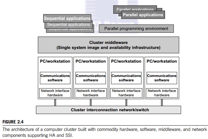
single job management system.
Single memory may be realized with the help of the compiler or a runtime
library. A single process space is not necessarily supported.
In
general, an idealized cluster is supported by three subsystems. First,
conventional databases and OLTP monitors offer users a desktop environment in
which to use the cluster. In addition to running sequential user programs, the
cluster supports parallel programming based on standard languages and
communication libraries using PVM, MPI, or OpenMP. The programming environment
also includes tools for debugging, profiling, monitoring, and so forth. A user
interface sub-system is needed to combine the advantages of the web interface
and the Windows GUI. It should also provide user-friendly links to various
programming environments, job management tools, hypertext, and search support
so that users can easily get help in programming the computer cluster.
1.2
Resource Sharing in Clusters
Supporting clusters of
smaller nodes will increase computer sales. Clustering improves both
avail-ability and performance. These two clustering goals are not necessarily
in conflict. Some HA clusters use hardware redundancy for scalable performance.
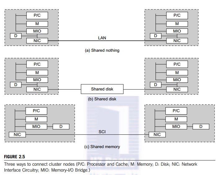
The nodes of a cluster can be connected in one of three ways, as shown in
Figure 2.5. The shared-nothing architecture is used in most clusters, where the
nodes are connected through the I/O bus. The shared-disk architecture is in
favor of small-scale availability
clusters in business applications. When one node fails, the other node
takes over.
The
shared-nothing configuration in Part (a) simply connects two or more autonomous
computers via a LAN such as Ethernet. A shared-disk cluster is shown in Part
(b). This is what most business clusters desire so that they can enable
recovery support in case of node failure. The shared disk can hold checkpoint
files or critical system images to enhance cluster availability. Without shared
disks, checkpointing, rollback recovery, failover, and failback are not
possible in a cluster. The shared-memory cluster in Part (c) is much more
difficult to realize. The nodes could be connected by a scalable coherence interface (SCI) ring, which is connected to
the memory bus of each node through an NIC module. In the other two
architectures, the interconnect is attached to the I/O bus. The memory bus
operates at a higher frequency than the I/O bus.
There is
no widely accepted standard for the memory bus. But there are such standards
for the I/O buses. One recent, popular standard is the PCI I/O bus standard.
So, if you implement an NIC card to attach a faster Ethernet network to the PCI
bus you can be assured that this card can be used in other systems that use PCI
as the I/O bus. The I/O bus evolves at a much slower rate than the memory bus.
Consider a cluster that uses connections through the PCI bus. When the
processors are upgraded, the interconnect and the NIC do not have to change, as
long as the new system still uses PCI. In a shared-memory cluster, changing the
processor implies a redesign of the node board and the NIC card.
2. Node Architectures and MPP
Packaging
In building large-scale clusters or MPP systems, cluster nodes are
classified into two categories: compute
nodes and service
nodes. Compute nodes appear in larger quantities
mainly used for large-scale searching or parallel floating-point computations.
Service nodes could be built with different processors mainly used to handle
I/O, file access, and system monitoring. For MPP clusters, the
compute nodes dominate in system cost, because
we may have 1,000 times more compute nodes than service nodes in a single large
clustered system. Table 2.3 introduces two example compute node architectures: homogeneous design and hybrid
node design.
In the past, most MPPs are built with a homogeneous architecture by
interconnecting a large number of the same compute nodes. In 2010, the Cray XT5
Jaguar system was built with 224,162 AMD Opteron processors with six cores
each. The Tiahe-1A adopted a hybrid node design using two Xeon CPUs plus two
AMD GPUs per each compute node. The GPU could be replaced by special
floating-point accelerators. A homogeneous node design makes it easier to
program and maintain the system.
Example
2.1 Modular Packaging of the IBM Blue Gene/L System
The Blue Gene/L is a supercomputer jointly developed by IBM and Lawrence
Livermore National Labora-tory. The system became operational in 2005 with a
136 Tflops performance at the No. 1 position in the
Top-500 list—toped the Japanese Earth Simulator. The system was upgraded
to score a 478 Tflops speed in 2007. By examining the architecture of the Blue
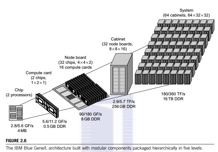
Gene series, we reveal the modular construction of a scalable MPP system as
shown in Figure 2.6. With modular packaging, the Blue Gene/L system is
con-structed hierarchically from processor chips to 64 physical racks. This
system was built with a total of 65,536 nodes with two PowerPC 449 FP2
processors per node. The 64 racks are interconnected by a huge 3D 64 x 32 x 32
torus network.
In the lower-left corner, we see a dual-processor chip. Two
chips are mounted on a computer card. Sixteen computer cards (32 chips or 64
processors) are mounted on a node board. A cabinet houses 32 node boards with
an 8 x 8 x 16 torus interconnect. Finally, 64 cabinets (racks) form the total
system at the upper-right corner. This packaging diagram corresponds to the
2005 configuration. Cus-tomers can order any size to meet their computational
needs. The Blue Gene cluster was designed to achieve scalable performance,
reliability through built-in testability, resilience by preserving locality of
failures and checking mechanisms, and serviceability through partitioning and
isolation of fault locations.
3. Cluster System Interconnects
3.1
High-Bandwidth Interconnects
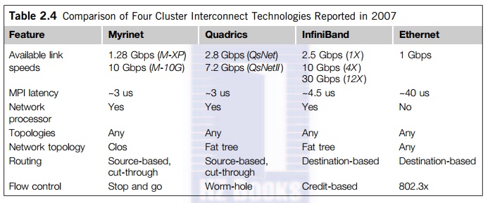
Table 2.4 compares four families of
high-bandwidth system interconnects. In 2007, Ethernet used a 1 Gbps link,
while the fastest InfiniBand links ran at 30 Gbps. The Myrinet and Quadrics
perform in between. The MPI latency represents the state of the art in
long-distance message passing. All four technologies can implement any network
topology, including crossbar switches, fat trees, and torus networks. The InfiniBand
is the most expensive choice with the fastest link speed. The Ethernet is still
the most cost-effective choice. We consider two example cluster interconnects
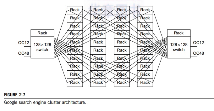
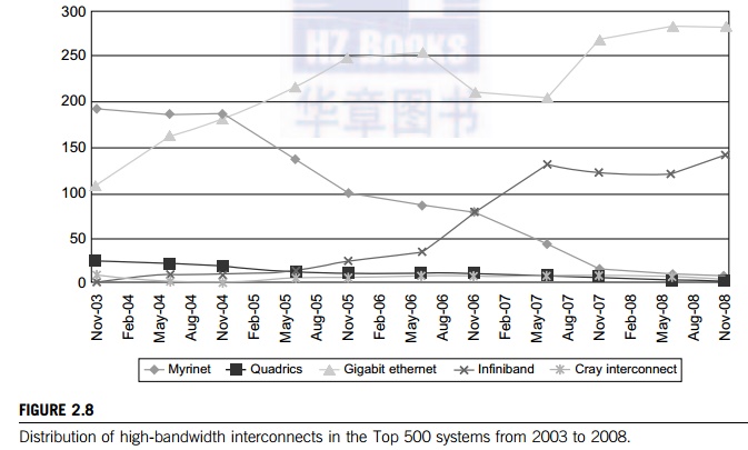
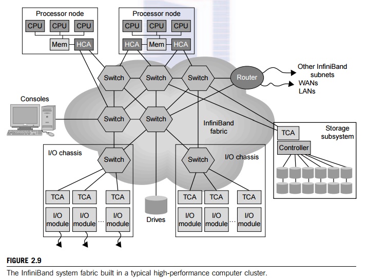
over 1,024 nodes in Figure 2.7 and Figure 2.9. The popularity of five cluster
interconnects is compared in Figure 2.8.
Example 2.2 Crossbar Switch in Google Search
Engine Cluster
Google
has many data centers using clusters of low-cost PC engines. These clusters are
mainly used to support Google’s web search business. Figure 2.7 shows a Google
cluster interconnect of 40 racks of PC engines via two racks of 128 x 128
Ethernet switches. Each Ethernet switch can handle 128 one Gbps Ethernet links.
A rack contains 80 PCs. This is an earlier cluster of 3,200 PCs. Google’s
search engine clusters are built with a lot more nodes. Today’s server clusters
from Google are installed in data centers with container trucks.
Two
switches are used to enhance cluster availability. The cluster works fine even
when one switch fails to provide the links among the PCs. The front ends of the
switches are connected to the Internet via 2.4 Gbps OC 12 links. The 622 Mbps
OC 12 links are connected to nearby data-center networks. In case of failure of
the OC 48 links, the cluster is still connected to the outside world via the OC
12 links. Thus, the Google cluster eliminates all single points of failure.
3.2
Share of System Interconnects over Time
Figure 2.8 shows the distribution of
large-scale system interconnects in the Top 500 systems from 2003 to 2008.
Gigabit Ethernet is the most popular interconnect due to its low cost and
market readiness. The InfiniBand network has been chosen in about 150 systems
for its high-bandwidth performance. The Cray interconnect is designed for use
in Cray systems only. The use of Myrinet and Quadrics networks had declined
rapidly in the Top 500 list by 2008.
Example 2.3 Understanding the InfiniBand
Architecture
The InfiniBand has a switch-based
point-to-point interconnect architecture. A large InfiniBand has a layered
architecture. The interconnect supports the virtual interface architecture
(VIA) for distributed mes-saging. The InfiniBand switches and links can make up
any topology. Popular ones include crossbars, fat trees, and torus networks.
Figure 2.9 shows the layered construction of an InfiniBand network. According
to Table 2.5, the InfiniBand provides the highest speed links and the highest
bandwidth in reported large-scale systems. However, InfiniBand networks cost
the most among the four interconnect technologies.
Each end point can be a storage controller, a
network interface card (NIC), or an interface to a host system. A host channel
adapter (HCA) connected to the host processor through a standard peripheral
component inter-connect (PCI), PCI extended (PCI-X), or PCI express bus
provides the host interface. Each HCA has more than one InfiniBand port. A
target channel adapter (TCA) enables I/O devices to be loaded within the
network. The TCA includes an I/O controller that is specific to its particular
device’s protocol such as SCSI, Fibre Channel, or Ethernet. This architecture
can be easily implemented to build very large scale cluster interconnects that
con-nect thousands or more hosts together. Supporting the InfiniBand in cluster
applications can be found in.
4. Hardware, Software, and Middleware
Support
Realistically, SSI and HA
features in a cluster are not obtained free of charge. They must be sup-ported
by hardware, software, middleware, or OS extensions. Any change in hardware
design and OS extensions must be done by the manufacturer. The hardware and OS
support could be cost-prohibitive to ordinary users. However, programming level
is a big burden to cluster users. There-fore, the middleware support at the
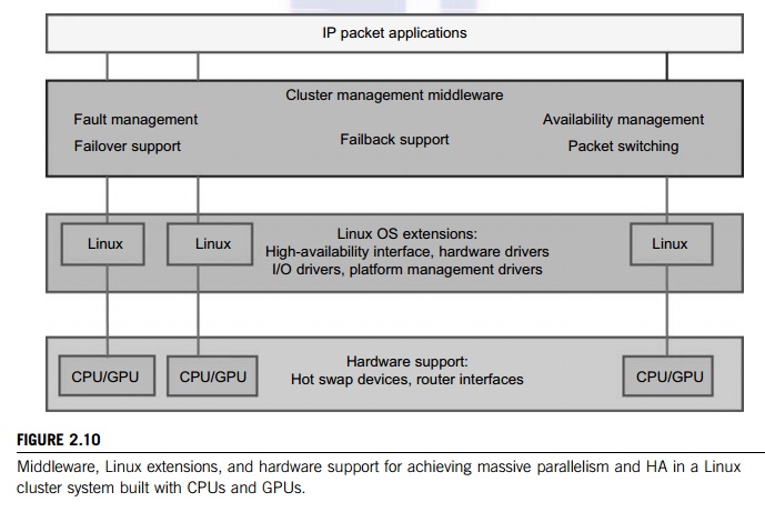
application level costs the least to implement. As an example, we show in
Figure 2.10 the middleware, OS extensions, and hardware support needed to
achieve HA in a typical Linux cluster system.
Close to
the user application end, middleware packages are needed at the cluster
management level: one for fault management to support failover and failback, to be discussed in Section 2.3.3. Another
desired feature is to achieve HA using failure detection and recovery and
packet switching. In the middle of Figure 2.10, we need to modify the Linux OS
to support HA, and we need special drivers to support HA, I/O, and hardware
devices. Toward the bottom, we need special hardware to support hot-swapped
devices and provide router interfaces. We will discuss various supporting
mechanisms in subsequent sections.
5. GPU Clusters for Massive
Parallelism
Commodity GPUs are becoming high-performance
accelerators for data-parallel computing. Modern GPU chips contain hundreds of
processor cores per chip. Based on a 2010 report [19], each GPU
chip is capable of achieving
up to 1 Tflops for single-precision (SP) arithmetic, and more than 80 Gflops
for double-precision (DP) calculations. Recent HPC-optimized GPUs contain up to
4 GB of on-board memory, and are capable of sustaining memory bandwidths
exceeding 100 GB/second. GPU clusters are built with a large number of GPU
chips. GPU clusters have already demonstrated their capability to achieve
Pflops performance in some of the Top 500 systems. Most GPU clusters are
structured with homogeneous GPUs of the same hardware class, make, and model.
The software used in a GPU cluster includes the OS, GPU drivers, and clustering
API such as an MPI.
The high
performance of a GPU cluster is attributed mainly to its massively parallel
multicore architecture, high throughput in multithreaded floating-point
arithmetic, and significantly reduced time in massive data movement using large
on-chip cache memory. In other words, GPU clusters already are more
cost-effective than traditional CPU clusters. GPU clusters result in not only a
quantum jump in speed performance, but also significantly reduced space, power,
and cooling demands. A GPU cluster can operate with a reduced number of
operating system images, compared with CPU-based clusters. These reductions in
power, environment, and management complexity make GPU clusters very attractive
for use in future HPC applications.
5.1
The Echelon GPU Chip Design
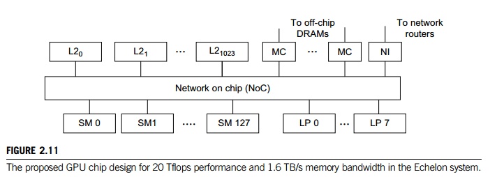
Figure 2.11 shows the
architecture of a future GPU accelerator that was suggested for use in
build-ing a NVIDIA Echelon GPU cluster for Exascale computing. This Echelong
project led by Bill Dally at NVIDIA is partially funded by DARPA under the Ubiquitous
High-Performance Computing (UHPC) program. This GPU design incorporates 1024
stream cores and 8 latency-optimized CPU-like cores (called latency processor)
on a single chip. Eight stream cores form a stream multi-processor (SM) and there are 128 SMs in
the Echelon GPU chip.
Each SM is designed with 8 processor cores to
yield a 160 Gflops peak speed. With 128 SMs, the chip has a peak speed of 20.48
Tflops. These nodes are interconnected by a NoC (network on chip) to 1,024 SRAM
banks (L2 caches). Each cache band has a 256 KB capacity. The MCs (memory controllers) are used to connect to
off-chip DRAMs and the NI (network
interface) is to scale the size of the GPU cluster
hierarchically, as shown in Figure 2.14. At the time of this writing, the
Echelon is only a research project. With permission from Bill Dally, we present
the design for
academic interest to
illustrate how one can explore the many-core GPU technology to achieve Exascale
computing in the future GPU technology to achieve Exascale computing in the
future.
5.2
GPU Cluster Components
A GPU cluster is often built as a heterogeneous
system consisting of three major components: the CPU host nodes, the GPU nodes
and the cluster interconnect between them. The GPU nodes are formed with
general-purpose GPUs, known as GPGPUs, to carry out numerical calculations. The
host node controls program execution. The cluster interconnect handles
inter-node communications. To guarantee the per-formance, multiple GPUs must be
fully supplied with data streams over high-bandwidth network and memory. Host memory
should be optimized to match with the on-chip cache bandwidths on the GPUs.
Figure 2.12 shows the proposed Echelon GPU clusters using the GPU chips shown
in Figure 2.11 as building blocks interconnected by a hierarchically
constructed network.
5.3
Echelon GPU Cluster Architecture
The Echelon system architecture is shown in Figure 2.11,
hierarchically. The entire Echelon system is built with N cabinets, labeled C0, C1, ... , CN. Each cabinet is built with 16 compute module
labeled as M0, M1, ... , M15. Each compute module is built with 8 GPU nodes
labeled as N0, N1, ... , N7. Each GPU node is the innermost block labeled as PC
in Figure 2.12 (also detailed in Figure 2.11).
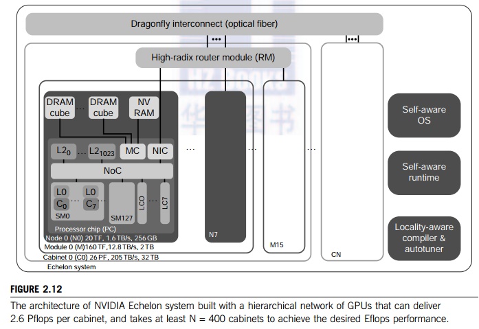
Each compute module features
a performance of 160 Tflops and 12.8 TB/s over 2 TB of memory. Thus, a single
cabinet can house 128 GPU nodes or 16,000 processor cores. Each cabinet has the
potential to deliver 2.6 Pflops over 32 TB memory and 205 TB/s bandwidth. The N cabinets are interconnected by a Dragonfly network
with optical fiber.
To
achieve Eflops performance, we need to use at least N = 400 cabinets. In total, an Exascale system
needs 327,680 processor cores in 400 cabinets. The Echelon system is supported
by a self-aware OS and runtime system. The Echelon system is also designed to
preserve locality with the support of compiler and autotuner. At present,
NVIDIA Fermi (GF110) chip has 512 stream proces-sors. Thus the Echelon design
is about 25 times faster. It is highly likely that the Echelon will employ
post-Maxwell NVIDIA GPU planned to appear in 2013 ~ 2014 time frame.
5.4
CUDA Parallel Programming
CUDA (Compute Unified Device Architecture) offers a parallel computing
architecture developed by NVIDIA. CUDA is the computing
engine in NVIDIA GPUs. This software is accessible to developers through
standard programming languages. Programmers use C for CUDA C with NVIDIA
extensions and certain restrictions. This CUDA C is compiled through a
PathScale Open64 C com-piler for parallel execution on a large number of GPU
cores. Example 2.4 shows the advantage of using CUDA C in parallel processing.
Example 2.4 Parallel SAXPY Execution Using CUDA
C Code on GPUs
SAXPY is a kernel operation frequently
performed in matrix multiplication. It essentially performs repeated mul-tiply
and add operations to generate the dot product of two long vectors. The
following saxpy_serial
routine is written in standard C code. This code is only suitable for
sequential execution on a single processor core.
Void
saxpy_serial (int n, float a, float*x, float *
{ for
(int i = 0; i < n; ++i), y[i] = a*x[i] + y[i] }
//
Invoke the serial SAXPY kernel
saxpy_serial
(n, 2.0, x, y);
The
following saxpy_parallel routine is written in CUDA C code for parallel execution by 256
threads/block on many processing cores on the GPU chip. Note that n blocks are handled by n pro-cessing cores, where n could be on the order of
hundreds of blocks.
_global__void
saxpy_parallel (int n, float a, float*x, float *y)
{ Int i
= blockIndex.x*blockDim.x + threadIndex.x; if (i < n) y [i] = a*x[i] + y[i]
}
// Invoke the parallel SAXPY kernel with 256 threads/block int
nblocks = (n + 255)/256; saxpy_parallel <<< nblocks, 256 >>>
(n, 2.0, x, y);
This is
a good example of using CUDA C to exploit massive parallelism on a cluster of
multi-core and multithreaded processors using the CODA GPGPUs as building
blocks.
5.5 CUDA Programming Interfaces
CUDA architecture shares a range of
computational interfaces with two competitors: the Khronos Group’s Open Computing Language and Microsoft’s
DirectCompute. Third-party wrappers are
also available for using Python, Perl, FORTRAN, Java, Ruby, Lua, MATLAB, and
IDL. CUDA has been used to accelerate nongraphical applications in
computational biology, cryptography, and other fields by an order of magnitude
or more. A good example is the BOINC distributed computing cli-ent. CUDA
provides both a low-level API and a higher-level API. CUDA works with all
NVIDIA GPUs from the G8X series onward, including the GeForce, Quadro, and
Tesla lines. NVIDIA states that programs developed for the GeForce 8 series
will also work without modification on all future NVIDIA video cards due to
binary compatibility.
5.6
Trends in CUDA Usage
Tesla and Fermi are two generations of CUDA
architecture released by NVIDIA in 2007 and 2010, respectively. The CUDA
version 3.2 is used for using a single GPU module in 2010. A newer CUDA version
4.0 will allow multiple GPUs to address use an unified virtual address space of
shared memory. The next NVIDIA GPUs will be Kepler-designed to support C++. The
Fermi has eight times the peak double-precision floating-point performance of
the Tesla GPU (5.8 Gflops/W versus 0.7 Gflops/W). Currently, the Fermi has up
to 512 CUDA cores on 3 billion transistors.
Future applications of the CUDA GPUs and the
Echelon system may include the following:
• The search for extraterrestrial intelligence
(SETI@Home)
• Distributed calculations to predict the native
conformation of proteins
• Medical analysis simulations based on CT and
MRI scan images
• Physical simulations in fluid dynamics and
environment statistics
• Accelerated 3D graphics, cryptography,
compression, and interconversion of video file formats
• Building the single-chip
cloud computer (SCC) through virtualization
in many-core architecture.
Related Topics