Chapter: Microprocessor and Microcontroller : 8086 System Bus Structure
Basic configurations: Read Write Timing Diagram
Basic
configurations : Read Write Timing Diagram
ü General Bus Operation
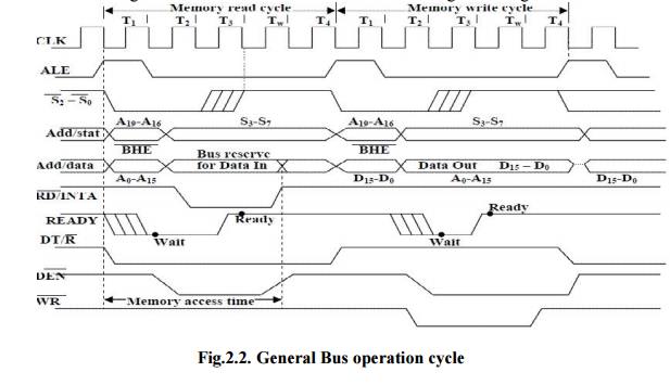
The 8086
has a combined address and data bus commonly referred as a time multiplexed
address and data bus. The main reason behind multiplexing address and data over
the same pins is the maximum utilization of processor pins and it facilitates
the use of 40 pin standard DIP package. The bus can be demultiplexed using a
few latches and transreceivers, whenever required.
Basically,
all the processor bus cycles consist of at least four clock cycles. These are
referred to as T1, T2, T3, T4. The address is transmitted by the processor
during T1, It is present on the bus only for one cycle. The negative edge of
this ALE pulse is used to separate the address and the data or status
information.
In
maximum mode, the status lines S0, S1 and S2 are used to indicate the type of
operation. Status bits S3 to S7 are multiplexed with higher order address bits
and the BHE signal. Address is valid during T1 while status bits S3 to S7 are
valid during T2 through T4.
System Bus timings: Minimum mode 8086 system and
timings
System
Design using 8086: Maximum mode 8086 system and timings
Related Topics