Operation, Major components | Special Function IC - Switching Regulators | Linear Integrated Circuits : Waveform Generators and Special Function ICs
Chapter: Linear Integrated Circuits : Waveform Generators and Special Function ICs
Switching Regulators
Switching
Regulators
Introduction
The
switching regulator offers the advantages
·
higher
power conversion efficiency
·
Increased
design flexibility (multiple output voltages of different polarities can be
generated from a single input voltage).
·
a
lot less heat and
·
Smaller
size.
The
primary filter capacitor is placed on the input to the regulator to help filter
out the 60 cycle ripple. If the output voltage is 12 volts and the input
voltage is 24 volts then we must drop 12 volts across the regulator. At output
currents of 10 amps this translates into 120 watts (12 volts times 10 amps) of
heat energy that the regulator must dissipate into heat.
The
switching regulator is much more efficient than the linear regulator achieving
efficiencies as high as 80% to 95% in some circuits. The obvious result is
smaller heat sinks, less heat and smaller overall size of the power supply.
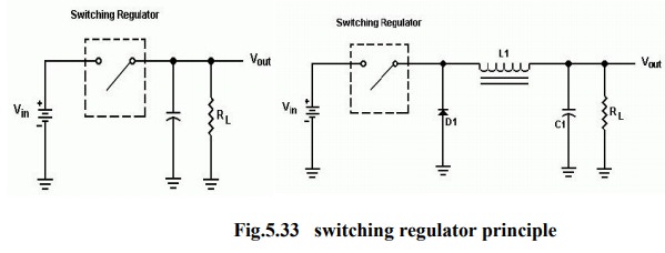
The
switching regulator is really nothing more than just a simple switch. This
switch goes on and off at a fixed rate usually between 50 Khz to 100Khz as set
by the circuit.
Operation:
Diode
D1 has to be a Schottky or other very fast switching diode. Inductor L1must be
a type of core that does not saturate under high currents. Capacitor C1 is
normally a low ESR (Equivalent Series Resistance) type.
To
understand the action of D1 and L1, let’s look at what happens when S1 is
closed as indicated below:
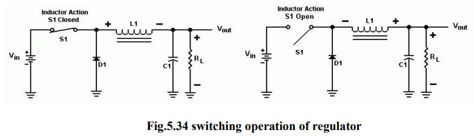
L1,
which tends to oppose the rising current, begins to generate an electromagnetic
field in its core. Diode D1 is reversed biased and is essentially an open
circuit at this point.
When
S1 opens, the electromagnetic field that was built up in L1 is now discharging
and generating a current in the reverse polarity. As a result, D1 is now
conducting and will continue until the field in L1 is diminished. This action
is similar to the charging and discharging of capacitor C1. The use of this
inductor/diode combination gives us even more efficiency and augments the
filtering of C1.
Because
the switching system operates in the 50 to 100 kHz region and has an almost
square waveform, it is rich in harmonics way up into the HF and even the
VHF/UHF region Four most commonly used switching converter types:
Buck:
used the reduce a DC voltage to a lower DC voltage.
Boost:
provides an output voltage that is higher than the input.
Buck-Boost
(invert): an output voltage is generated opposite in polarity to the input.
Fly
back: an output voltage that is less than or greater than the input can be
generated, as well as multiple outputs.
Converters:
Push-Pull:
A two-transistor converter that is especially efficient at low input voltages.
Half-Bridge:
A two-transistor converter used in many off-line applications. Full-Bridge: A
four-transistor converter (usually used in off-line designs) that can generate
the highest output power of all the types listed.
Switching Regulator:
An
example of general purpose regulator is Motorola’s MC1723. It can be used in
many different ways, for example, as a fixed positive or negative output
voltage regulator, variable regulator or switching regulator because of its
flexibility.
To
minimize the power dissipation during switching, the external transistor used
must be a switching power transistor.
To
improve the efficiency of a regulator, the series pass transistor is used as a
switch rather than as a variable resistor as in the linear mode.
·
A
regulator constructed to operate in this manner is called a series switching
regulator. In such regulators the series pass transistor is switched between
cut off & saturation at a high frequency which produces a pulse width
modulated (PWM) square wave output.
·
This
output is filtered through a low pass LC filter to produce an average dc output
voltage.
·
Thus
the output voltage is proportional to the pulse width and frequency.
·
The
efficiency of a series switching regulator is independent of the input &
output differential & can approach 95%
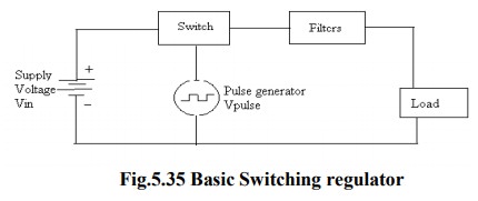
A
basic switching regulator consists of 4 major components,
1.
Voltage
source Vin
2.
Switch
S1
3.
Pulse
generator Vpulse
4. Filter F1
1.
Voltage Source Vin:
It
may be any dc supply – a battery or an unregulated or a regulated voltage. The
voltage source must satisfy the following requirements.
·
It
must supply the required output power & the losses associated with the
switching regulator.
·
It
must be large enough to supply sufficient dynamic range for line & load
regulations.
·
It
must be sufficiently high to meet the minimum requirement of the regulator
system to be designed.
· It may be required to store energy for a specified amount of time during power failures.
2. Switch S1:
It
is typically a transistor or thyristor connected as a power switch & is
operated in the saturated mode. The pulse generator output alternately turns
the switch ON & OFF
3. Pulse generator Vpulse:
It
provides an asymmetrical square wave varying in either frequency or pulse width
called frequency modulation or pulse width modulation respectively. The most
effective frequency range for the pulse generator for optimum efficiency 20
KHz. This frequency is inaudible to the human ear & also well within the
switching speeds of most inexpensive transistors & diodes.
·
The
duty cycle of the pulse wave form determines the relationship between the input
& output voltages. The duty cycle is the ratio of the on time ton, to the
period T of the pulse waveform.
Duty
cycle = ton/(ton+toff) = ton/T =ton.f
Where
ton
= On-time of the pulse waveform toff=off-time of the pulse wave form
T
= time period = ton + toff
=1/frequency
or T = 1/f
·
Typical
operating frequencies of switching regulator range from 10 to 50 kHz.
·
Lower
operating frequency improve efficiency & reduce electrical noise, but
require large filter components (inductors & capacitors).
3.
Filter F1:
It
converts the pulse waveform from the output of the switch into a dc voltage.
Since this switching mechanism allows a conversion similar to transformers, the
switching regulator is often referred to as a dc transformer.
The
output voltage Vo of the switching regulator is a function of duty cycle &
the input voltage Vin.
Vo
is expressed as follows,
Vo=
ton Vin/T
·
This
equation indicates that, if time period T is constant, Vo is directly
proportional to the ON-time, ton for a given value of Vin. This method of
changing the output voltage by varying ton is referred to as a pulse width
modulation.
·
Similarly,
if ton is held constant, the output voltage Vo is inversely proportional to the
period T or directly proportional to the frequency of the pulse waveform. This
method of varying the output voltage is referred to as frequency modulation
(FM).
·
Switching
regulator can operate in any of 3 modes
i)
Step
– Down
ii) Step – Up
iii) Polarity inverting
Related Topics