Chapter: Basic Electrical and Electronics Engineering : Digital Electronics
SR, JK and Master-Slave JK Flip-Flop
SR Flip-Flop
An SR Flip-Flop can be considered as a
basic one-bit memory device that has two inputs, one which will "SET"
the device and another which will "RESET" the device back to its
original state and an output Q that will be either at a logic level
"1" or logic "0" depending upon this Set/Reset condition. A
basic NAND Gate SR flip flop circuit provides feedback from its outputs to its
inputs and is commonly used in memory circuits to store data bits. The term
"Flip-flop" relates to the actual operation of the device, as it can
be "Flipped" into one logic state or "Flopped" back into
another.
The
simplest way to make any basic one-bit Set/Reset SR flip-flop is to connect
together a pair of cross-coupled 2-input NAND Gates to form a Set-Reset
Bistable or a SR NAND Gate Latch, so that there is feedback from each output to
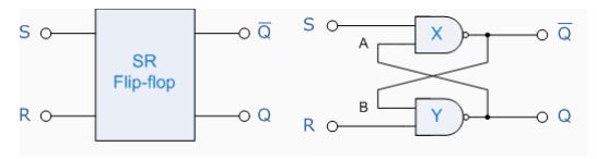
one of the other NAND Gate inputs. This device consists of two inputs, one
called the Reset, R and the other called the Set, S with two corresponding
outputs Q and its inverse or complement Q as shown below.
The SR NAND Gate Latch
The Set State
Consider
the circuit shown above. If the input R is at logic level "0" (R = 0)
and input S is at logic level "1" (S = 1), the NAND Gate Y has at least one of its inputs at
logic "0" therefore, its output Q must be at a logic level
"1" (NAND Gate principles). Output Q is also fed back to input A and
so both inputs to the NAND Gate X
are at logic level "1", and therefore its output Q must be at logic
level "0". Again NAND gate principals. If the Reset input R changes
state, and now becomes logic "1" with S remaining HIGH at logic level
"1", NAND Gate Y inputs
are now R = "1" and B = "0" and since one of its inputs is
still at logic level "0"
the output at Q remains at logic level "1" and the circuit is said to
be "Latched" or "Set" with Q = "1" and Q =
"0".
Reset State
In this
second stable state, Q is at logic level "0", Q = "0" its
inverse output Q is at logic level "1", not Q = "1", and is
given by R = "1" and S = "0". As gate X has one of its inputs at logic "0" its output Q must
equal logic level "1" (again NAND gate principles). Output Q is fed
back to input B, so both inputs to NAND gate Y are at logic "1", therefore, Q = "0". If the
set input, S now changes state to logic "1" with R remaining at logic
"1", output Q still remains LOW at logic level "0" and the
circuit's "Reset" state has been latched.
Truth Table for this Set-Reset
Function
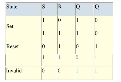
It can be
seen that when both inputs S = "1" and R = "1" the outputs
Q and Q can be at either logic level "1" or "0", depending
upon the state of inputs S or R BEFORE this input condition existed. However,
input state R = "0" and S = "0" is an undesirable or
invalid condition and must be avoided because this will give both outputs Q and
Q to be at logic level "1" at the same time and we would normally
want Q to be the inverse of Q. However, if the two inputs are now switched HIGH
again after this condition to logic "1", both the outputs will go LOW
resulting in the flip-flop becoming unstable and switch to an unknown data
state based upon the unbalance. This unbalance can cause one of the outputs to
switch faster than the other resulting in the flip-flop switching to one state
or the other which may not be the required state and data corruption will
exist. This unstable condition is known as its Meta-stable state.
Then, a
bistable latch is activated or Set by a logic "1" applied to its S
input and deactivated or Reset by a logic "1" applied to its R. The
SR Latch is said to be in an "invalid" condition (Meta-stable) if
both the Set and Reset inputs are activated simultaneously.
As well
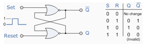
as using NAND Gates, it is also possible to construct simple 1-bit SR Flip-flops
using two NOR Gates connected the same configuration. The circuit will work in a similar way to the NAND
gate circuit above, except that the invalid condition exists when both its
inputs are at logic level "1" and this is shown below.
The NOR Gate SR Flip-flop
The JK Flip-Flop
From the
previous tutorial we now know that the basic gated SR NAND Flip-flop suffers from two basic problems: Number 1, the S
= 0 and R = 0 condition or S = R = 0 must always be avoided, and number 2, if S
or R change state while the enable input is high the correct latching action
will not occur. Then to overcome these two problems the JK Flip-Flop was
developed.
The JK
Flip-Flop is basically a Gated SR Flip-Flop with the addition of clock input
circuitry that prevents the illegal or invalid output that can occur when both
input S equals logic level "1" and input R equals logic level
"1". The symbol for a JK Flip-flop is similar to that of an SR
Bistable as seen in the previous tutorial except for the addition of a clock
input.
The JK Flip-flop
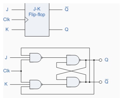
Both the
S and the R inputs of the previous SR bistable have now been replaced by two
inputs called the J and K inputs, respectively. The two 2-input NAND gates of
the gated SR bistable have now been replaced by two 3-input AND gates with the
third input of each gate connected to the outputs Q and Q. This cross coupling
of the SR Flip-flop allows the previously invalid condition of S =
"1" and R = "1" state to be usefully used to turn it into a
"Toggle action" as the two inputs are now interlocked. If the circuit
is "Set" the J input is
inhibited by the "0" status of the Q through the lower AND gate. If
the circuit is "Reset" the
K input is inhibited by the "0" status of Q through the upper AND
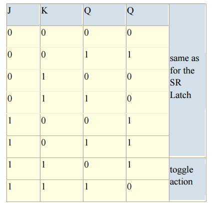
gate. When both inputs J and K are equal to logic "1", the JK
flip-flop changes state and the truth table for this is given below.
The Truth Table for the JK
Function
Then the
JK Flip-flop is basically an SR Flip-flop with feedback and which enables only
one of its two input terminals, either Set or Reset at any one time thereby
eliminating the invalid condition seen previously in the SR Flip-flop circuit.
Also when both the J and the K inputs are at logic level "1" at the
same time, and the clock input is pulsed either "HIGH" or
"LOW" the circuit will "Toggle" from a Set state to a Reset
state, or visa-versa. This results in the JK Flip-flop acting more like a T-type Flip-flop when both terminals
are "HIGH".
Although
this circuit is an improvement on the clocked SR flip-flop it still suffers
from timing problems called "race" if the output Q changes state
before the timing pulse of the clock input has time to go "OFF". To
avoid this the timing pulse period (T) must be kept as short as possible (high
frequency). As this is sometimes is not possible with modern TTL IC's the much
improved Master-Slave JK Flip-flop was
developed. This eliminates all the timing
problems by using two SR flip-flops connected together in series, one for
the "Master" circuit, which triggers on the leading edge of the clock
pulse and the other, the "Slave" circuit, which triggers on the
falling edge of the clock pulse.
Master-Slave JK Flip-flop
The Master-Slave Flip-Flop is basically two
JK bistable flip-flops connected together in a series configuration with the
outputs from Q and Q from the "Slave" flip-flop being fed back to the
inputs of the "Master" with the outputs of the "Master"
flip-flop being connected to the two inputs of the "Slave" flip-flop as
shown below.
Master-Slave JK Flip-Flops
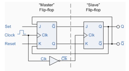
The input
signals J and K are connected to the "Master" flip-flop which
"locks" the input while the clock (Clk) input is high at logic level
"1". As the clock input of the "Slave" flip-flop is the
inverse (complement) of the "Master" clock input, the outputs from
the "Master" flip-flop are only "seen" by the
"Slave" flip-flop when the clock input goes "LOW" to logic
level "0". Therefore on the "High-to-Low" transition of the
clock pulse the locked outputs of the "Master" flip-flop are fed
through to the JK inputs of the "Slave" flip-flop making this type of
flip-flop edge or pulse-triggered.
Then, the
circuit accepts input data when the clock signal is "HIGH", and
passes the data to the output on the falling-edge of the clock signal. In other
words, the Master-Slave JK Flip-flop is
a "Synchronous" device as it only passes data with the timing of the clock signal.
Related Topics