Chapter: Electronic Circuits : Biasing of Discrete BJT and MOSFET
Load line and Variation of quiescent point
Load line and Variation of
quiescent point
Biasing
is the application of dc voltages to establish a fixed level of current and
voltage. For transistor amplifiers the resulting dc current and voltage
establish an operating point on the characteristics that define the region that
will be employed for amplification of the applied signal. Since the operating point
is a fixed point on the characteristics, it is also called the quiescent point
(abbreviated Q-point). The operating point of a device, also known as bias point,
quiescent point, or Q-point, is the point on the output characteristics that
shows the DC collector–emitter voltage (Vce) and the collector
current (Ic) with no input signal applied.
Consider
the fixed bias circuit,
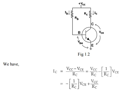
We can
draw a straight line on the graph of IC versus VCE which
is having slope -1/Rc.To determine the two points on the line we assume VCE
= VCC and VCE =0
a) When VCE =VCC ; IC
=0 and we get a point A
b) When VCE=0 ; IC=VCC/RC and we get a point B
The
figure below shows the output characteristic curves for the transistor in CE
mode. The DC load line is drawn on the output characteristic curves. Load line - To draw load line, we have
to find saturation current and the cutoff voltage.
Saturation point - The point
at which the load line intersects the characteristic curve near thecollector
current axis is referred to as the saturation
point . At this point of time, the current through the transistor is
maximum and the voltage across collector is minimum for a given value of load.
So, saturation current for the fixed bias circuit, Ic (sat) =Vcc/Rc .
Cutoff point -The point where the load line
intersects the cutoff region of the collector curvesis referred as the cutoff
point (i.e. end of load line). At this point, collector current is
approximately zero and emitter is grounded for fixed bias circuit. so, Vce (cut) = Vc = VccOperating point -
The "Q point" for a
transistor amplifier circuit is the point along itsoperating region in a
"quiescent ", where no input signal gets amplified.
The
figure below shows the output characteristic curves for the transistor in CE
mode with points A and B, and line drawn between them. The line drawn between
points A and B is called d.c load line. The d.c word indicates that only d.c
conditions are considered, i.e input signal is assumed to be zero.
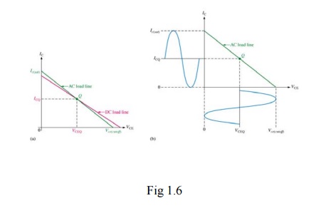
The d.c
load line is a plot of IC versus VCE. For a given value
of Rc and a given value of Vcc. So, it represents all collector current levels
and corresponding collector emitter voltages that can exist in the circuit.
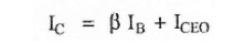
Knowing any one of Ic, IB, or VCE , it is easy to
determine the other two from the load line. The slope of the d.c load line
depends on the value of RC. It is the negative and equal to
reciprocal of the RC.
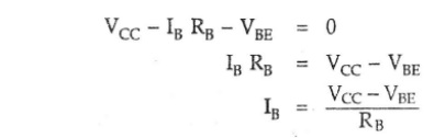
Applying
KVL to the base circuit, we get
The
intersection of curves of different values IB of with d.c load line
gives different operating points. For different values of IB, we
have different intersection points such as P, Q and R.
Selection of operating point
The
operating point can be selected at different positions on the d.c load line,
near saturation region, near cut-off region or at the centre, i.e in the active
region. The selection of operating point will depend on its application. When
transistor is used as an amplifier, the Q point should be selected at the
center of the d.c. load line to prevent any possible distortion in the
amplified output signal.
Case 1
Biasing
circuit is designed to fix a Q point at point P which is very near to the
saturation region. It results collector current is clipped at the positive half
cycle. i.e. distortion is present at the output. Therefore, point P is not a
suitable operating point.
Case 2
Biasing
circuit is designed to fix a Q point at point R as shown in Fig. Point R is very
near to the cut-off region. Here, the collector current is clipped at the
negative half cycle. So, point R is also not a suitable operating point.
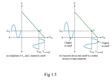
Case 3
Biasing
circuit is designed to fix a Q point at point Q as shown in Fig.. The output
signal is sinusoidal waveform without any distortion. Thus point Q is the best
operating point.
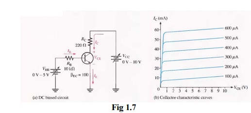
The
figure 1.7 shows the biasing of transistor in common emitter configuration.
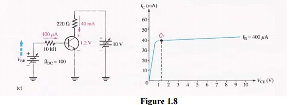
In Figure
1.8, we assign three values to IB and observe what happens to IC
and VCE. First, VBB is adjusted to produce an IB
of 200 A, as shown in Figure 1.8(a), Since IC = βDC IB,
the collector current is 20 mA, as indicated, and
VCE
= VCC - IcRc = 10 V - (20 mA) (220 Ω) = 10 V - 4.4 V = 5.6 V This
Q-point is shown on the graph of Figure 1.3(b) as Q1.
Next, as
shown in Figure 1.8(b), VBB is increased to produce an IB
of 300 µA and an Ic of 30mA.
VCE
= 10 V - (30 mA) (220 Ω) = 10V – 6.6 V = 3.4 V
The
Q-point for this condition is indicated by Q2 on the graph.
Finally.as
in Figure 1.8 (c), VBB is increased to give an IB of 400
µA and an Ic of 40 mA.
VCE
= 10 V - (40 mA) (220 Ω) = 10 V - 8.8 V = 1.2 V Q3 is the corresponding Q-point
on the graph.
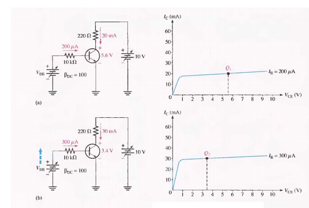
Notice
that when IB increases, Ic increases and VCE decreases.
When IB decreases, Ic decreases and VCE increases. As VBB
is adjusted up or down, the dc operating point of the transistor moves along a
sloping straight line, called the DC load line, connecting each separate
Q-point.
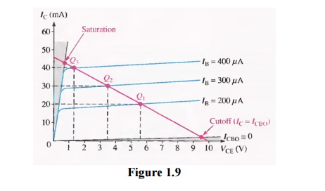
At any
point along the line, values of IB, Ic, and VCE can be
picked off the graph, as shown in Figure1.9.
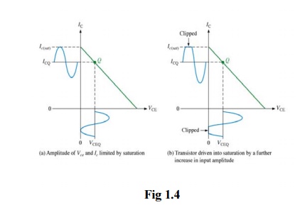
The dc
load line intersects the VCE axis at 10 V. The point where VCE
= VCC. This is the transistor cutoff point because IB and
IC are zero (ideally). Actually, there is a small leakage current, ICBO
, at cutoff as indicated, and therefore VCE is slightly less than 10
V but normally this can be neglected.
The dc
load line intersects the IC axis at 45.5 mA ideally. This is the
transistor saturation point because IC is maximum at the point where
VCE = 0 V and IC = VCC / RC.
Actually,
there is a small voltage (VCE (sat)) across the transistor, and I C(sat)
is slightly less than 45.5 mA, as indicated in Figure 1.4. Note that
Kirchhoff's voltage law applied around the collector loop gives,
VCC - ICRC - VCE
= 0.
These
results in a straight line equation for the load line of the form y = mx + b as follow:
IC = - (1/RC) VCE
+VCC / RC
Where, - (1/RC)
is the slope and VCC/ RC
is the y-axis intercept point.
Variation of quiescent point due to hFE
variation within manufacturers tolerance
It is
clear that the biasing circuit should be designed to fix the operating point or
Q point at the center of the active region. But only fixing of the operating
point is not sufficient. While designing the biasing circuit, care should be
taken so that the operating point will not shift into an undesirable region
(i.e. into cut-off or saturation region). Designing the biasing circuit to
stabilize the Q point is known as bias stability.
Two
important factors are to be considered while designing the biasing circuits
which are responsible for, shifting the operating point.
I. Temperature
1)
Ico: The
flow of current in the circuit produces heat at the junctions. This
heatincreases the temperature at the junctions". We know that the minority
carriers are temperature dependent. They increase with the temperature. The
increase in the minority carriers increases
the leakage current ICE0,

Specifically,
ICB0 doubles for every 10°C rise in temperature. Increase in ICE0
in turn increases the collector current
The
increase in IC further raises the temperature at the collector
junction and the same cycle repeats. This excessive increase in IC
shifts the operating point into the saturation region, changing the operating
condition set by biasing circuit.
As the
power dissipated within a transistor is predominantly the Power dissipated at
its collector base junction, the power dissipation is given as

The
increase in the collector current increases the power dissipated at the
collector junction. This, in turn further increases the temperature of the
junction and hence increases the collector current. The process is cumulative.
The excess heat produced at the collector base junction may even burn and
destroy the transistor. This situation is called 'Thermal runaway’ of the
transistor. For any transistor, maximum Power dissipation is always a fixed
value. That is known as maximum power dissipation rating of a transistor. This
value is specified by the manufacturer in data sheet. If this limit is crossed,
the device will fail.
2) VBE: Base to emitter voltage VBEchanges
with temperature at the rate of 2.5mV/°CBase current, IB depends
upon VBE .As base current IB depends on VBE,
and Ic depends on IB, Ic depends on VBE. Therefore
collector current Ic. Change with temperature due to change in VBE.
The change in collector current change the operating point.
3)βdc:βdc of the transistor is also
temperature dependent. Asβdc varies, Ic alsovaries, since Ic = βIB.
The change in collector current change the operating point.
Therefore,
to avoid thermal instability, the biasing circuit should be designed to provide
a degree of temperature stability i.e. even though there are temperature
changes, the changes in the transistor parameters (VCE , I CQ
, PDmax )should be very less so that the operating point shifting is
minimum in the middle of the active region.
II) Transistor current gain hFE/β
Eventhough
there is tremendous advancement in semiconductor technology, there are changes
in the transistor parameters among different units of the same type, same
number. This means if we take two transistor units of same fire (i.e. same
number, construction, parameter specified etc.) and use them in the circuit,
there is change in the β value in actual practice. The biasing circuit is
designed according to the required β
value. But due to change in β from unit to unit, the operating point may shift
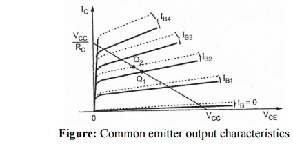
Figure shows the common emitter output characteristics for
two transistors of the same type. The dashed characteristics are for a
transistor whose p is much larger than that of the transistor represented by
the solid curves.
So for
stabilizing the operating point the factors discussed so far should be
considered while designing the biasing circuit.
Related Topics