Chapter: Digital Electronics : Sequential Circuits
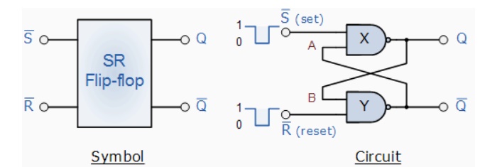
SR Flip Flop
SR FLIP-FLOP:
The SR flip-flop can be considered as one of the most basic sequential logic circuit possible. The flip-flop is basically a one-bit memory bistable device that has two inputs, one which will "SET" the device (meaning the output = "1"), and is labelled S and another which will "RESET" the device (meaning the output = "0"), labelled R. Then the SR description stands for set/reset. The reset input resets the flip-flop back to its original state with an output Q that will be either at a logic level "1" or logic "0" depending upon this set/reset condition.
A basic NAND gate SR flip-flop circuit provides feedback from both of its outputs back to its inputs and is commonly used in memory circuits to store data bits. Then the SR flip-flop actually has three inputs, Set, Reset and its current output Q relating to it's current state or history. The term "Flip-flop" relates to the actual operation of the device, as it can be "flipped" into one logic state or "flopped" back into another.
1.THE NAND GATE SR FLIP-FLOP:
The simplest way to make any basic one-bit set/reset SR flip-flop is to connect together a pair of cross-coupled 2-input NAND gates to form a set-reset bistable or an active LOW SR NAND Gate Latch, so that there is feedback from each output to one of the other NAND gate inputs. This device consists of two inputs, one called the set, S and the other called the reset, R with two corresponding outputs Q and its inverse or complement Q as shown below.
The Basic SR Flip-flop
The Set State
Consider the circuit shown above. If the input R is at logic level "0" (R = 0) and input S is at logic level "1" (S = 1), the NAND gate Y has at least one of its inputs at logic "0" therefore, its output Q must be at a logic level "1" (NAND Gate principles). Output Q is also fed back to input "A" and so both inputs to NAND gate X are at logic level "1", and therefore its output Q must be at logic level "0". Again NAND gate principals. If the reset input R changes state, and goes HIGH to logic "1" with S remaining HIGH also at logic level "1", NAND gate Y inputs are now R = "1" and B = "0". Since one of its inputs is still at logic level "0" the output at Q still remains HIGH at logic level "1" and there is no change of state. Therefore, the flip-flop circuit is said to be "Latched" or "Set" with Q = "1" and Q = "0".
Reset State
In this second stable state, Q is at logic level "0", not Q = "0" its inverse output Q is at logic level "1", Q = "1", and is given by R = "1" and S = "0". As gate X has one of its inputs at logic "0" its output Q must equal logic level "1" (again NAND gate principles). Output Q is fed back to input "B", so both inputs to NAND gate Y are at logic "1", therefore, Q = "0". If the set input, S now changes state to logic "1" with input R remaining at logic "1", output Q still remains LOW at logic level "0" and there is no change of state. Therefore, the flip-flop circuits "Reset" state has been latched. We can define this "set/reset" action in the following truth table.
Truth Table for this Set-Reset Function
It can be seen that when both inputs S = "1" and R = "1" the outputs Q and Q can be at either logic level "1" or "0", depending upon the state of inputs S or R BEFORE this input condition existed. However, input state R = "0" and S = "0" is an undesirable or invalid condition and must be avoided because this will give both outputs Q and Q to be at logic level "1" at the same time and we would normally want Q to be the inverse of Q. However, if the two inputs are now switched HIGH again after this condition to logic "1", both the outputs will go LOW resulting in the flip-flop becoming unstable and switch to an unknown data state based upon the unbalance. This unbalance can cause one of the outputs to switch faster than the other resulting in the flip-flop switching to one state or the other which may not be the required state and data corruption will exist. This unstable condition is known as its Meta-stable state.
Then, a bistable SR flip-flop or SR latch is activated or set by a logic "1" applied to its S input and deactivated or reset by a logic "1" applied to its R. The SR flip-flop is said to be in an "invalid" condition (Meta-stable) if both the set and reset inputs are activated simultaneously.
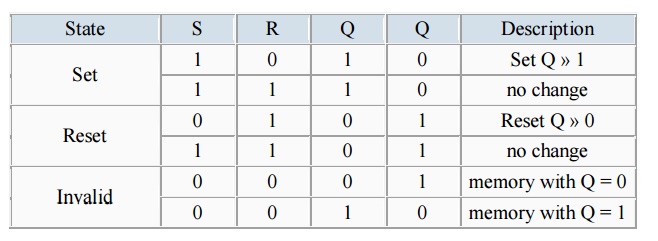
As well as using NAND gates, it is also possible to construct simple one-bit SR Flip-flops using two cross-coupled NOR gates connected in the same configuration. The circuit will work in a similar way to the NAND gate circuit above, except that the inputs are active HIGH and the invalid condition exists when both its inputs are at logic level "1", and this is shown below.
The NOR Gate SR Flip-flop
2. SWITCH DEBOUNCE CIRCUITS:
Edge-triggered flip-flops require a nice clean signal transition, and one practical use of this type of set-reset circuit is as a latch used to help eliminate mechanical switch "bounce". As its name implies, switch bounce occurs when the contacts of any mechanically operated switch, push-button or keypad are operated and the internal switch contacts do not fully close cleanly, but bounce together first before closing (or opening) when the switch is pressed. This gives rise to a series of individual pulses which can be as long as tens of milliseconds that an electronic system or circuit such as a digital counter may see as a series of logic pulses instead of one long single pulse and behave incorrectly. For example, during this bounce period the output voltage can fluctuate wildly and may register multiple input counts instead of one single count. Then set-reset SR Flip-flops or Bistable Latch circuits can be used to eliminate this kind of problem and this is demonstrated below.
SR Bistable Switch Debounce Circuit
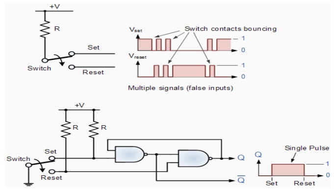
Depending upon the current state of the output, if the set or reset buttons are depressed the output will change over in the manner described above and any additional unwanted inputs (bounces) from the mechanical action of the switch will have no effect on the output at Q. When the other button is pressed, the very first contact will cause the latch to change state, but any additional mechanical switch bounces will also have no effect. The SR flip-flop can then be RESET automatically after a short period of time, for example 0.5 seconds, so as to register any additional and intentional repeat inputs from the same switch contacts, for example multiple inputs from a keyboards "RETURN" key.
Commonly available IC's specifically made to overcome the problem of switch bounce are the MAX6816, single input, MAX6817, dual input and the MAX6818 octal input switch debouncer IC's. These chips contain the necessary flip-flop circuitry to provide clean interfacing of mechanical switches to digital systems.
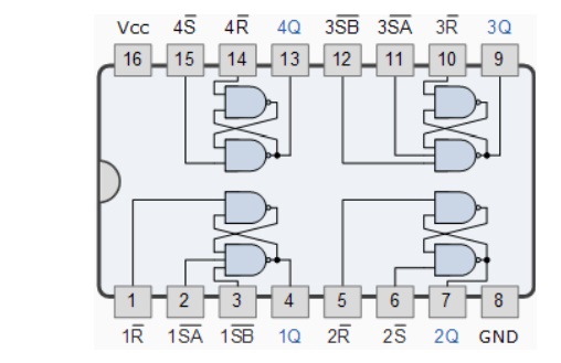
Set-Reset bistable latches can also be used as Monostable (one-shot) pulse generators to generate a single output pulse, either high or low, of some specified width or time period for timing or control purposes. The 74LS279 is a Quad SR Bistable Latch IC, which contains four individual NAND type bistable's within a single chip enabling switch debounce or monostable/astable clock circuits to be easily constructed.
Quad SR Bistable Latch 74LS279
3. GATED OR CLOCKED SR FLIP-FLOP:
It is sometimes desirable in sequential logic circuits to have a bistable SR flip-flop that only changes state when certain conditions are met regardless of the condition of either the Set or the Reset inputs. By connecting a 2-input AND gate in series with each input terminal of the SR Flip-flop a Gated SR Flip-flop can be created. This extra conditional input is called an "Enable" input and is given the prefix of "EN". The addition of this input means that the output at Q only changes state when it is HIGH and can therefore be used as a clock (CLK) input making it level-sensitive as shown below.
Gated SR Flip-flop
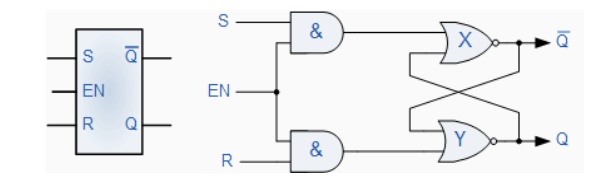
When the Enable input "EN" is at logic level "0", the outputs of the two AND gates are also at logic level "0", (AND Gate principles) regardless of the condition of the two inputs S and R, latching the two outputs Q and Q into their last known state. When the enable input "EN" changes to logic level "1" the circuit responds as a normal SR bistable flip-flop with the two AND gates becoming transparent to the Set and Reset signals. This enable input can also be connected to a clock timing signal adding clock synchronisation to the flip-flop creating what is sometimes called a "Clocked SR Flip-flop". So a Gated Bistable SR Flip-flop operates as a standard bistable latch but the outputs are only activated when a logic "1" is applied to its EN input and deactivated by a logic "0".
In the next tutorial about Sequential Logic Circuits, we will look at another type of edge-triggered flip-flop which is very similar to the RS flip-flopcalled a JK Flip-flop named after its inventor, Jack Kilby. The JK flip-flop is the most widely used of all the flip-flop designs as it is considered to be a universal device.
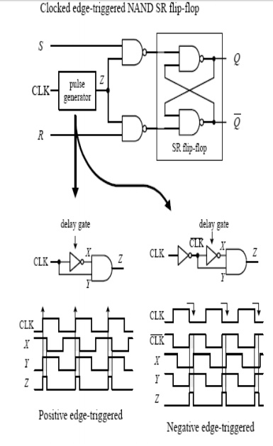
4. EDGE-TRIGGERED SR FLIP-FLOPS:
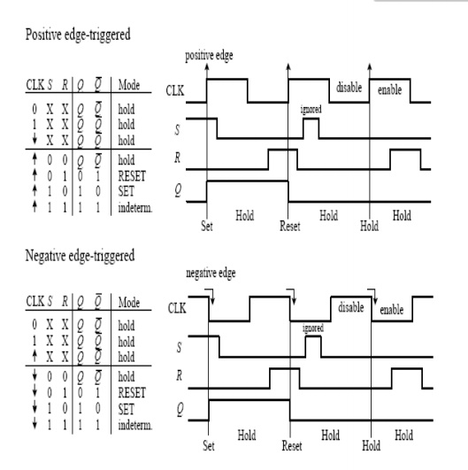
Now there is an annoying feature with the last level-triggered flip-flop; its S and R inputs have to be held at the desired input condition (set, reset, no change) for the entire time that the clock signal is enabling the flip-flop. With a slight alteration, however, you can make the level-triggered flip-flop more flexible (in terms of timing control) by turning it into an edge-triggered flip-flop. An edge-triggered flipflop samples the inputs only during either a positive or negative clock edge (↑ = positive edge, ↓ = negative edge).
Any changes that occur before or after the clock edge are ignored—the flip-flop will be placed in hold mode. To make an edgetriggered flip-flop, introduce either a positive or a negative level-triggered clock pulse generator network into the previous level-triggered flip-flop, as shown in Fig.In a positive edge-triggered generator circuit, a NOT gate with propagation delay is added.
Since the clock signal is delayed through the inverter, the output of the AND gate will not provide a low (as would be the case without a propagation delay) but will provide a pulse that begins at the positive edge of the clock signal and lasts for a duration equal to the propagation delay of the NOT gate. It is this pulse that is used to clock the flip-flop. Within the negative edge-triggered generator network, the clock signal is first inverted and then applied through the same NOT/AND network.
The pulse begins at the negative edge of the clock and lasts for a duration equal to the propagation delay of the NOT gate. The propagation delay is typically so small (in nanoseconds) that the pulse is essentially an “edge.”
Related Topics