Chapter: RF and Microwave Engineering : Microwave Tubes and Measurements
Operation of Multicavity Klystron
OPERATION OF MULTICAVITY KLYSTRON
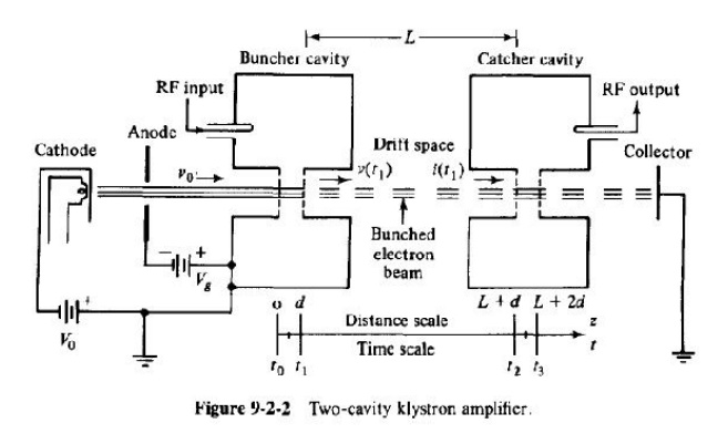
Two cavity klystron:
The two-cavity klystron is a widely used
microwave amplifier operated by the principles of velocity and current
modulation. All electrons injected from the cathode arrive at the first cavity
with uniform velocity. Those electrons passing the first cavity gap at zeros of
the gap voltage (or signal voltage) pass through with unchanged velocity; those
passing through the positive half cycles of the gap voltage undergo an increase
in velocity; those passing through the negative swings of the gap voltage
undergo a decrease in velocity.
As a result of these actions, the electrons
gradually bunch together as they travel down the drift space. The variation in
electron velocity in the drift space is known as velocity modulation. The density of the electrons in the second
cavity gap varies cyclically with time.
The electron beam contains an ac component and
is said to be current-modulated. The maximum bunching should occur
approximately midway between the second cavity grids during its retarding
phase; thus the kinetic energy is transferred from the electrons to the field
of the second cavity.
The electrons then emerge from the second
cavity with reduced velocity and finally terminate at the collector. The
charateristics of a two-cavity klystron amplifier are as follows:
1.Efficiency: about 40%.
2.Power output: average power ( CW power) is up
to 500 kW and pulsed power is up to 30 MW at 10 GHz.
3.Power gain: about 30 dB.
Reentrant Cavities
The coaxial cavity is similar to a coaxial line
shorted at two ends and joined at the center by a capacitor. The input
impedance to each shorted coaxial line is given by
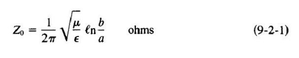
where e is the length of the coaxial line.
Substitution of Eq. (9-2-l) in (9-2-2) results in
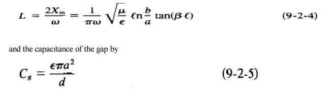
The inductance of the cavity is given by
At resonance the inductive reactance of the two
shorted coaxial lines in series is equal in magnitude to the capacitive
reactance of the gap. That is, wL =
1/(wCg).
Thus where v
= 1/yr;;; is the phase velocity in any medium
Velocity-Modulation
Process
When electrons are first accelerated by the
high de voltage Vo before entering
the buncher grids, their velocity is uniform:
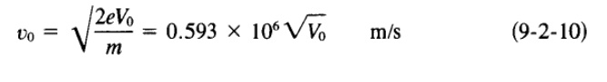
In Eq. (9-2-10) it is assumed that electrons
leave the cathode with zero velocity. When a microwave signal is applied to the
input terminal, the gap voltage between the buncher grids appears as
where V1 is the amplitude of the signal and V1
<< Vo is assumed.
In order to find the modulated velocity in the
buncher cavity in terms of either the entering time to or the exiting time t1 and the gap transit angle 88 as shown in Fig. 9-2-2 it is
necessary to determine the average microwave voltage in the buncher gap as
indicated in Fig. 9-2-6. Since V1 << Vo
, the average transit time through the buncher gap distance d is
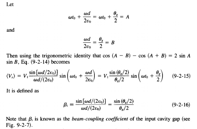
It can be seen that increasing the gap transit
angle 0g decreases the coupling
between the electron beam and the buncher cavity; that is, the velocity
modulation of the beam for a given microwave signal is decreased. Immediately
after velocity modulation, the exit velocity from the buncher gap is given by
Bunching Process
Once the electrons leave the buncher cavity,
they drift with a velocity given by Eq. (9-2-19) or (9-2-20) along in the
field-free space between the two cavities. The effect of velocity modulation
produces bunching of the electron beam-or current modulation.
The electrons that pass the buncher at Vs = 0 travel through with unchanged
velocity vo and become the bunching
center. Those electrons that pass the buncher cavity during the positive half
cycles of the microwave input voltage Vs
travel faster than the electrons that passed the gap when Vs = 0. Those electrons that pass the buncher cavity during the
negative half cycles of the voltage Vs
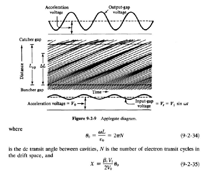
travel slower than the electrons that passed the gap when Vs = 0. At a distance of !:J..L
along the beam from the buncher cavity, the beam electrons have drifted into
dense clusters. Figure 9-2-8 shows the trajectories of minimum, zero, and
maximum electron acceleration.
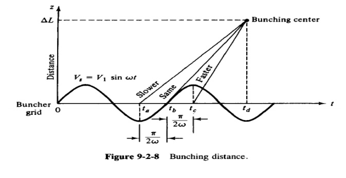
The distance from the buncher grid to the location of dense electron bunching for the electron at tb is

Related Topics