Chapter: Computer Architecture : Memory and I/O Systems
Memory Technologies
MEMORY TECHNOLOGIES
Memory latency is traditionally
quoted using two measures—access time and cycle time. Access time is the time
between when a read is requested and when the desired word arrives, cycle time
is the minimum time between requests to memory. One reason that cycle time is
greater than access time is that the memory needs the address lines to be
stable between accesses.
DRAM technology
The main memory of
virtually every desktop or server computer sold since 1975 is composed of
semiconductor DRAMs,. As early DRAMs grew in capacity, the cost of a package
with all the necessary address lines was an issue. The solution was to
multiplex the
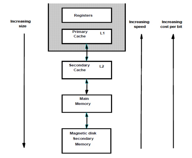
Fig5.1
DRAM technology
address lines, thereby cutting the number of address
pins in half. One half of the address is sent first, called the row access
strobe or(RAS). It is followed by the other half of the address, sent during
the column access strobe(CAS). These names come from the internal chip
organization, since the memory is organized as a rectangular matrix addressed
by rows and columns.
DRAMs are commonly sold
on small boards called DIMMs for Dual Inline Memory Modules. DIMMs typically
contain 4 to 16 DRAMs. They are normally organized to be eight bytes wide for
desktop systems.
SRAM Technology
In contrast to DRAMs
are SRAMs—the first letter standing for static. The dynamic nature of the
circuits in DRAM require data to be written back after being read, hence the difference
between the access time and the cycle time as well as the need to refresh.
SRAMs typically use six transistors per bit to prevent the information from
being disturbed when read.
In DRAM designs the
emphasis is on cost per bit and capacity, while SRAM designs are concerned with
speed and capacity. (Because of this concern, SRAM address lines are not
multiplexed.). Thus, unlike DRAMs, there is no difference between access time
and cycle time. For memories designed in comparable technologies, the capacity
of DRAMs is roughly 4 to 8 times that of SRAMs. The cycle time of SRAMs is 8 to
16 times faster than DRAMs, but they are also 8 to 16 times as expensive.
Embedded Processor Memory Technology:
ROM and Flash
Embedded computers
usually have small memories, and most do not have a disk to act as non-volatile
storage. Two memory technologies are found in embedded computers to address
this problem.
The first is Read-Only
Memory (ROM). ROM is programmed at time of manufacture, needing only a single
transistor per bit to represent 1 or 0. ROM is used for the embedded program
and for constants, often included as part of a larger chip.In addition to being
non-volatile, ROM is also non-destructible; nothing the computer can do can
modify the contents of this memory. Hence, ROM also provides a level of
protection to the code of embedded computers. Since address based protection is
often not enabled in embedded processors, ROM can fulfill an important role.
The second memory
technology offers non-volatility but allows the memory to be modified. Flash
memory allows the embedded device to alter nonvolatile memory after the system
is manufactured, which can shorten product development.
Improving Memory Performance in a
standard DRAM Chip
To improve bandwidth, there have been a variety of
evolutionary innovations over time.
1.
The first was timing signals that allow
repeated accesses to the row buffer without another row access time, typically
called fast page mode..
2.
The second major change is that
conventional DRAMs have an asynchronousinterface to the memory controller, and
hence every transfer involves overhead to synchronize with the controller.This
optimization is called Synchronous DRAM( SDRAM).
3. The third major DRAM innovation to increase bandwidth is to transfer data onboth the rising edge and falling edge of the DRAM clock signal, thereby doubling the peak data rate. This optimization is calledDouble Data Rate(DDR).
Related Topics