Chapter: Microprocessor and Microcontroller : I/O Interfacing
Memory Interfacing and I/O interfacing
Memory Devices and Interfacing
Any application of a microprocessor based system
requires the transfer of data between external circuitry to the microprocessor
and microprocessor to the external circuitry. Most of the peripheral devices
are designed and interfaced with a CPU either to enable it to communicate with
the user or an external process and to ease the circuit operations so that the
microprocessor works more efficiently.
The use of peripheral integrated devices simplifies
both the hardware circuits and software considerable. The following are the
devices used in interfacing of Memory and General I/O devices
• 74LS138
(Decoder / Demultiplexer).
• 74LS373 /
74LS374 3-STATE Octal D-Type Transparent Latches.
• 74LS245
Octal Bus Transceiver: 3-State.
74LS138 (Decoder / Demultiplexer)
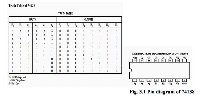
The LS138 is a high speed 1-of-8 Decoder/
Demultiplexer fabricated with the low power Schottky barrier diode process. The
decoder accepts three binary weighted inputs (A0, A1, A2) and when enabled
provides eight mutually exclusive active LOW Outputs (O0–O7).
The LS138
can be used as an 8-output demultiplexer by using one of the active LOW Enable
inputs as the data input and the other Enable inputs as strobes. The Enable
inputs which are not used must be permanently tied to their appropriate active
HIGH or active LOW state.
74LS373 / 74LS374 3-STATE Octal
D-Type Transparent Latches and Edge-Triggered Flip-Flops
These
8-bit registers feature totem-pole 3-STATE outputs designed specifically for
implementing buffer registers, I/O ports, bidirectional bus drivers, and
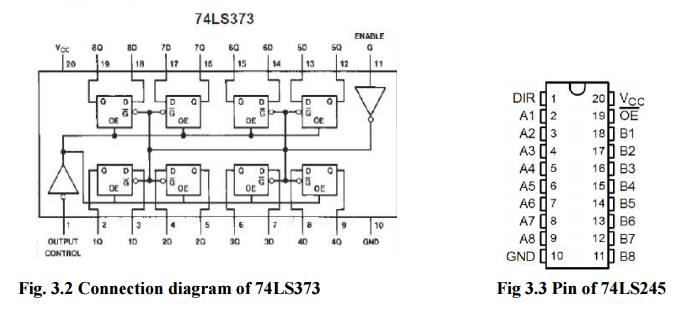
working registers. The eight latches of the 74LS373 are transparent D type
latches meaning that while the enable (G) is HIGH the Q outputs will follow the
data (D) inputs.
When the
enable is taken LOW the output will be latched at the level of the data that was
set up. The eight flip-flops of the 74LS374 are edge-triggered D-type flip
flops. On the positive transition of the clock, the Q outputs will be set to
the logic states that were set up at the D inputs.
Main Features
• Choice of
8 latches or 8 D-type flip-flops in a single package
• 3-STATE
bus-driving outputs
• Full
parallel-access for loading
• Buffered
control inputs
• P-N-P
inputs reduce D-C loading on data lines
74LS245 Octal Bus Transceiver:
3-State
The
74LS245 is a high-speed Si-gate CMOS device. The 74LS245 is an octal
transceiver featuring non- inverting 3-state bus compatible outputs in both
send and receive directions. The 74LS245 features an Output Enable (OE) input
for easy cascading and a send/receive (DIR) input for direction control. OE
controls the outputs so that the buses are effectively isolated. All inputs
have a Schmitt-trigger action.
These
octal bus transceivers are designed for asynchronous two-way communication
between data buses. The 74LS245 is a high-speed Si-gate CMOS device. The
74LS245 is an octal transceiver featuring non-inverting 3-state bus compatible
outputs in both send and receive directions.
The 74LS245
features an Output Enable (OE) input for easy cascading and a send/receive
(DIR) input for direction control. OE controls the outputs so that the buses
are effectively isolated. All inputs have a Schmitt-trigger action. These octal
bus transceivers are designed for asynchronous two-way communication between
data buses.
Memory Devices And Interfacing
The
memory interfacing circuit is used to access memory quit frequently to read
instruction codes and data stored in the memory. The read / write operations
are monitored by control
signals.
Semiconductor memories are of two types. Viz. RAM (Random Access Memory) and
ROM (Read Only Memory) The Semiconductor RAM’s are broadly two types-
static
Ram and dynamic RAM
Memory structure and its requirements
The read
/ write memories consist of an array of registers in which each register has
unique address. The size of memory is N * M as shown in figure.
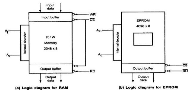
Where N
is number of register and M is the word length, in number of bits. As shown in
figure(a) memory chip has 12 address lines Ao–A11, one chip select
(CS), and two control lines, Read (RD) to enable output buffer and Write (WR)
to enable the input buffer.
The
internal decoder is used to decoder the address lines. Figure(b) shows the
logic diagram of a typical EPROM (Erasable Programmable Read-Only Memory) with
4096 (4K) register. It has 12 address lines Ao – A11, one chip select (CS), one read control signal. Since EPROM
does not require the (WR) signal.
EPROM (or
EPROMs) is used as a program memory and RAM (or RAMs) as a data memory. When
both, EPROM and RAM are used, the total address space 1 Mbytes is shared by
them.
Address Decoding Techniques
• Absolute
decoding
• Linear
decoding
• Block
decoding
Absolute Decoding:
In the
absolute decoding technique the memory chip is selected only for the specified
logic level on the address lines: no other logic levels can select the chip.
Below figure the memory interface with absolute decoding. Two 8K EPROMs (2764)
are used to provide even and odd memory banks. Control signals BHE and Ao are use to enable output of odd and
even memory banks respectively. As each memory chip has 8K memory locations,
thirteen address lines are required to address each locations, independently.
All remaining address lines are used to generate an unique chip select signal.
This address technique is normally used in large memory systems.
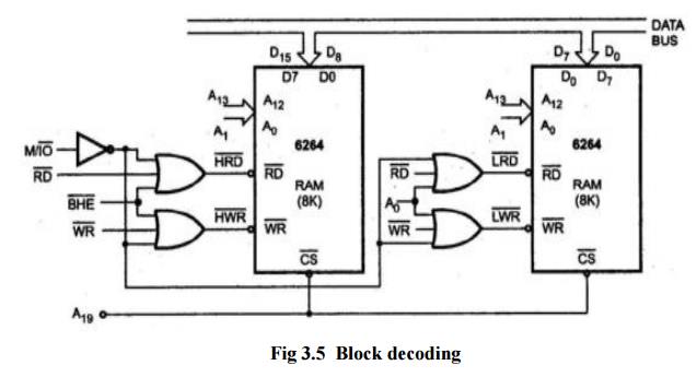
Linear Decoding:
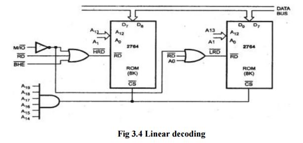
In small
system hardware for the decoding logic can be eliminated by using only required
number of addressing lines (not all). Other lines are simple ignored. This
technique is referred as linear decoding or partial decoding. Control signals
BHE and Ao are used to enable odd
and even memory banks, respectively. Figure shows the addressing of 16K RAM (6264)
with linear decoding. The address line A19
is used to select the RAM chips. When A19
is low, chip is selected, otherwise it is disabled. The status of A14 to A18 does not affect the chip selection logic. This gives you
multiple addresses (shadow addresses). This technique reduces the cost of
decoding circuit, but it gas drawback of multiple addresses
Block Decoding:
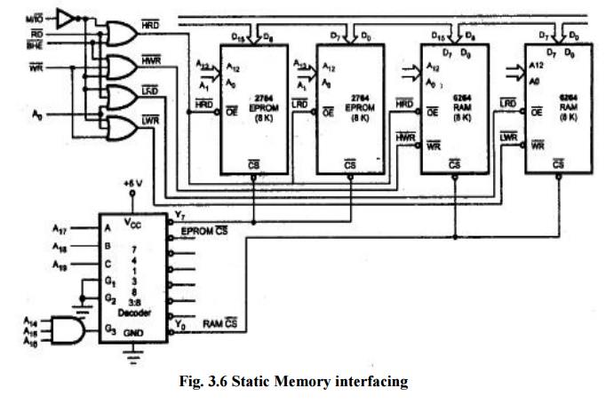
In a
microcomputer system the memory array is often consists of several blocks of
memory chips. Each block of memory requires decoding circuit. To avoid separate
decoding for each memory block special decoder IC is used to generate chip
select signal for each block.
Static Memory Interfacing
The
general procedure of static memory interfacing with 8086 as follows:
1. Arrange
the available memory chips so as to obtain 16-bit data bus width. The upper
8-bit bank is called ‘odd address memory bank’ and the lower 8-bit bank is
called ‘even address memory bank’.
2. Connect
available memory address lines of memory chips with those of the microprocessor
and also connect the memory RD and WR inputs to the corresponding processor
control signals. Connect the 16-bit data bus of the memory bank with that of
the microprocessor 8086.
3. The
remaining address lines of the microprocessor, BHE and Ao are used for decoding
the required chip select signals for the odd and even memory banks. The CS of
memory is derived from the output of the decoding circuit.
4. As a good
and efficient interfacing practice, the address map of the system should be
continuous as far as possible
Dynamic RAM Interfacing
The basic Dynamic RAM cell uses a capacitor to
store the charge as a representation of data. This capacitor is manufactured as
a diode that is reverse-biased so that the storage capacitance comes into the
picture. This storage capacitance is utilized for storing the charge
representation of data but the reverse-biased diode has a leakage current that
tends to discharge the capacitor giving rise to the possibility of data loss.
To avoid this possible data loss, the data stored
in a dynamic RAM cell must be refreshed after a fixed time interval regularly.
The process of refreshing the data in the RAM is known as refresh cycle. This
activity is similar to reading the data from each cell of the memory,
independent of the requirement of microprocessor, regularly. During this
refresh period all other operations (accesses) related to the memory subsystem
are suspended.
The advantages of dynamic RAM. Like low power
consumption, higher packaging density and low cost, most of the advanced
computer systems are designed using dynamic RAMs. Also the refresh mechanism
and the additional hardware required makes the interfacing hardware, in case of
dynamic RAM, more complicated, as compared to static RAM interfacing circuit.
Interfacing I/O Ports
I/O ports
or input/output ports are the devices through which the microprocessor
communicates with other devices or external data sources/destinations. Input
activity, as one may expect, is the activity that enables the microprocessor to
read data from external devices, for example keyboard, joysticks, mouser etc.
the devices are known as input devices as they feed data into a microprocessor
system.
Output activity transfers data from the microprocessor
top the external devices, for example CRT display, 7-segment displays, printer,
etc, the devices that accept the data from a microprocessor system are called
output devices.
Steps in Interfacing an I/O
Device
The
following steps are performed to interface a general I/O device with a CPU:
1. Connect
the data bus of the microprocessor system with the data bus of the I/O port.
2. Derive a
device address pulse by decoding the required address of the device and use it
as the chip select of the device.
3. Use a
suitable control signal, i.e. IORD and /or IOWR to carry out device operations,
i.e. connect IORD to RD input of the device if it is an input devise, otherwise
connect IOWR to WR input of the device. In some cases the RD or WR control
signals are combined with the device address pulse to generate the device
select pulse.
Input Port
The input
device is connected to the microprocessor through buffer. The simplest form of
a input port is a buffer as shown in the figure. This buffer is a tri-state
buffer and its output is available only when enable signal is active. When
microprocessor wants to read data from the input device (keyboard), the control
signals from the microprocessor activates the buffer by asserting enable input
of the buffer. Once the buffer is enabled, data from the device is available on
the data bus. Microprocessor reads this data by initiating read command.
Output Port
It is
used to send the data to the output device such as display from the
microprocessor. The simplest form of the output port is a latch.
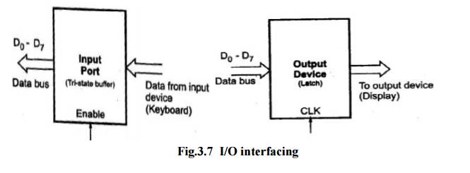
The
output device is connected to the microprocessor through latch as shown in the
figure. When microprocessor wants to send data to the output device it puts the
data on the data bus and activates the clock signal of the latch, latching the
data from the data bus at the output of latch. It is then available at the
output of latch for the output device.
I/O Interfacing Techniques
Input/output
devices can be interfaced with microprocessor systems in two ways:
1. I/O mapped
I/O
2. Memory
mapped I/O
1. I/O mapped I/O:
8086 has
special instructions IN and OUT to transfer data through the input/output ports
in I/O mapped I/O system. The IN instruction copies data from a port to the
Accumulator. If an 8-bit port is read data will go to AL and if 16-bit port is
read the data will go to AX. The OUT instruction copies a byte from AL or a
word from AX to the specified port. The M/IO signal is always low when 8086 is
executing these instructions. In this address of I/O device is 8-bit or 16-bit.
It is 8-bit for Direct addressing and 16-bit for Indirect addressing.
2. Memory mapped I/O
In this
type of I/O interfacing, the 8086 uses 20 address lines to identify an I/O
device. The I/O device is connected as if it is a memory device. The 8086 uses
same control signals and instructions to access I/O as those of memory, here RD
and WR signals are activated indicating memory bus cycle.
Related Topics